With the rapid development of the electronic information industry, digital technology and IC manufacturing technology, DAC has a good market environment in the digital background of information, such as mobile phone manufacturing, wireless networks and other fields. Therefore, DACs with good performance in terms of update rate and stability and power consumption will have better market prospects. Since the process technology has entered the nano-scale stage to this day, the development of the DAC has been greatly improved in terms of working speed and power consumption performance. In order to obtain a high-performance DAC, in addition to process manufacturing technology, the key lies in the stability of the bandgap reference source. Due to the low temperature coefficient of the bandgap reference, it is widely used in analog and mixed-signal circuits, so the reference voltage generated by the reference is related to the analog and digital signals. If the reference voltage produces a +1% error, the DAC analog output is increased by 1% because the analog output produced by the DAC is proportional to the product of the reference voltage and the input digital quantity. Therefore, the accuracy of the reference source must be better than the DAC design accuracy specification. It is necessary to design a voltage reference source with low power consumption, low temperature coefficient and high power supply rejection. To improve the performance of the reference source, reducing the error technique becomes the key. In terms of reducing power consumption, it is proposed to use all MOS transistors to operate in a sub-threshold state, thereby achieving low power consumption. It is also proposed to use a MOS tube with different conductive characteristics in different working areas to design a voltage reference source with full MOS structure. Although the performance of the reference source is greatly improved in terms of low power consumption, it is in terms of power supply rejection characteristics. Need to make adjustments and improvements. In order to improve the power supply voltage rejection ratio, it is proposed to use the basic principle of the bandgap voltage, combined with the self-bias current mirror and the appropriate startup circuit to obtain a voltage reference circuit with high power supply rejection ratio. It is also proposed to comprehensively consider the design circuit to eliminate the limitation of the offset voltage and voltage suppression ratio of the op amp in the traditional bandgap reference voltage source. The simulation results show that there is still room for improvement in circuit performance.
After combining the above methods, advantages and disadvantages of improving the performance of the bandgap reference voltage source and the practical application requirements of the DAC, this paper uses a 40 nm CMOS process. Based on the traditional design principle, in order to obtain a more stable PTAT current, negative feedback is utilized. The principle and the working mechanism of the basic current mirror, and the use of a proportional resistance value design to improve the stability of the circuit. In the layout design, in order to reduce the mismatch and layout area of ​​the MOS tube, the self-bias of the current mirror structure is replaced by a resistor, which makes the circuit structure simpler and more practical.
1 Basic design principle of bandgap referenceThe basic design principle of the traditional bandgap reference is to use the same characteristics of the positive and negative quiescent operating points of the op amp, and also to use the bipolar transistor VBE with a negative temperature coefficient and two different collector currents. The ΔVBE of a bipolar transistor has a positive temperature coefficient characteristic, and the design of a bandgap reference voltage source is completed by adjusting the magnitude of the resistance [8]. Based on the 40 nm CMOS process, a high stability bandgap reference circuit is designed. Figure 1 shows the actual circuit of a bandgap reference.

1.1 Reference core circuit diagram analysis
As shown in Figure 1, the overall architecture of the design can be seen, using the formula in [9] when the supply voltage and the effective enable signal are provided, and the entire bandgap reference is operating normally. Perform circuit analysis. The voltage drop across resistor R1 is:
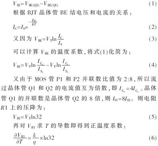
Since the VBE(Q1) of the BJT transistor has a negative temperature coefficient, the approximate negative temperature coefficient is -1.5 mV/K when VBE(Q1) is about 750 mV and T is 300 K; and ΔVBE has a positive temperature coefficient. At room temperature, it is about +0.087 mV/°C. Therefore, by appropriately selecting the resistance values ​​of R1 and R2, the sum of the two components can be brought to zero temperature coefficient, thereby obtaining a reference voltage with better temperature characteristics:

1.2 Startup circuit analysis
As shown in Figure 1, when the input supply voltage VDD is 2.5 V, when EN is low, nEN is high, and ENA is low. When the MOS transistor P9 is turned off, the operational amplifier circuit is provided without a bias current, and since the MOS transistors N3 and N4 are turned on, the N5 and N6 are short-circuited by the ground, that is, the entire operational amplifier circuit is in an inoperative state. Since P3 is turned on, the fb (feedback) signal is pulled up to VDD, which is high level, P11 is on, P10 is off due to nEN being high, N2 is on, and VDD and VSS are not shorted. Since the gate input of N1 is nEN, the Vref is pulled down to VSS, so the output voltage is low, and the op amp and V+, V- supply circuits are not working, so the bias current source and the reference core are turned off. When EN is high, nEN is low and ENA is high. The MOS transistor P9 is turned on to allow current to flow into the amplifier. When the current is stable, the op amp circuit is activated through resistor R3. At the same time, N3, N4, and P3 are turned off, and the reference core circuit can work normally. The MOS transistor N1 is in an off state, allowing normal Vref output. If en_vbg and envbg_z cause the transmission gate module to be in the off state, even if Vref has a normal output value, the final output signal vbg is also a low level voltage value. The startup circuit increases the stability and fault tolerance of the circuit itself; it also helps to reduce the power consumption of the DAC.
1.3 OPAMP actual circuit diagram analysis
The OPAMP actual circuit shown in Figure 1 is in the deep negative feedback state during normal operation, that is, the positive and negative input voltages are clamped at the same potential, which is fully utilized in the bandgap reference voltage source. This feature of the op amp is used to achieve temperature-independent bandgap voltage output [9]. This is a typical two-stage operational amplifier circuit structure, P5, P6 and N5, N6 and P9, R3 constitute the first stage, N7, N8 and P7, P8MOS tube constitutes the second stage. Among them, P9, N3 and N4 are switching tubes, which control the working state of the two-stage operational amplifiers. When P9 is turned on, the bias current is generated through the resistor R3. N3 and N5 are in the off state and the op amp can work normally. When the input port VDD is 2.5 V, the tested differential op amp has a gain of 67.8 dB, which meets the design requirements.
2 Simulation results and layout2.1 Layout and post-simulation results analysis
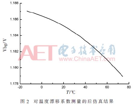
The actual circuit and layout and its front and back simulations are based on a 40 nm CMOS process, using cadence to simulate the circuit. Firstly, different test circuits are built for different test parameters, and then Spectre software is used for simulation [10]. The two clock control signals en_vbg and envbg_z of the transmission gate are set to low level and high level respectively to make the transmission gate open. Setting the enable signal EN to a low level allows the op amp and PTAT module to function properly. The power supply voltage VDD input is 2.5 V and the VSS input is 0 V. The test is performed with each module operating normally with a current of 156.74 μA, an output voltage of 1.184 V, and a startup time of 0.5 μs.
From Fig. 2, it can be seen that the power supply voltage is 2.5 μV, and the temperature varies linearly from -15 °C to 75 °C. The data obtained from the simulation results were calculated and the simulated temperature drift coefficient was 8.7×10⁻⁵/°C.
It can be seen from Fig. 3 that the PSRR is -85 dB at low frequency at room temperature, and the results show that the bandgap reference has good voltage suppression characteristics.

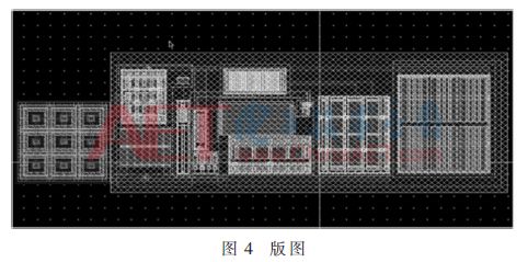
According to the design rules of the 40 nm process, the layout shown in Figure 4 is drawn. For the MOS tube with wide channel, the interdigital structure is drawn to reduce the influence of the process limitation on the circuit performance. For the differential op amp In order to reduce the input offset voltage, the layout is overall symmetrical; for better matching, the layout of the nine bipolar transistors is adjusted, and dummy MOS transistors are added around some devices.
2.2 Comparison and analysis with other literature parameters
It can be seen from Table 1 that the advantages and disadvantages of this paper are compared with the references. The disadvantages of temperature stability in this paper are particularly obvious. There are still many problems. It is necessary to improve the weight of positive temperature coefficient and negative temperature coefficient in the circuit. It has certain reference value in power supply suppression characteristics.
3 ConclusionThe accuracy of the reference source in this paper must be better than the DAC design accuracy specification. Using the principle of negative feedback and basic current mirror, a stable PTAT current is obtained under reasonable design of the circuit, and a high-precision and fast-start CMOS bandgap reference voltage is obtained according to the design principle of the bandgap reference voltage source. At the same time, in terms of layout area and circuit performance, in order to meet the requirements of the DAC index, try to reduce the number of MOS tubes used to reduce the generation of parasitic parameters in the layout, such as eliminating the use of self-bias current. MOS tube. Finally, a reference output voltage of 1.184 V, a startup time of 0.5 μs, a supply voltage rejection ratio of -85 dB, a layout area of ​​7531.9 μm 2 , and a bandgap reference that can be integrated into the high speed DAC chip are obtained. This bandgap reference is applied by a high speed, high resolution DA converter.

Whaylan portable power station, High capacity, high power, built-in lithium battery, long standby time, high conver-sion efficiency, easy to carry.Designed for comfortable handling, the WL-P300/600 is equipped with a top handle and the entire body is so light that even a small child can easily lift it. With its 311wh/540wh capacity, you can live off-grid anywhere, anytime, from RV camping to wilderness adventures, without fear of power outages.
Whaylan always adheres to the concept of "innovation drives development, science and technology leads the future", product research and development is quality oriented, efficiency-oriented, safety-oriented as a principle, creating a strong team, R&D experience, the company is rated as small and medium-sized scientific and technical enterprises, specialized new enterprises, high-tech enterprises.
Since its inception, the company has always adhered to the original intention of "allowing the world to use clean energy", dipped deep in the field of energy, electronic and electrical transformation, and is committed to providing smart energy management and other common solutions to households, industrial and commercial users and ground-based power plants with innovative technologies, excellent products and professional services.
In the context of the global energy revolution, Whaylan will continue to focus on the new business of energy equipment, research and innovation at all times, always close to the needs of users, and will strive to build a world-class green technology enterprise, create a new era of smart energy!
portabel power station,power station,camping power station,outdoor power station
suzhou whaylan new energy technology co., ltd , https://www.whaylan.com