1 Introduction
MEMS microphones are miniature sensors that convert audio signals into electrical signals, and their working process involves disciplines such as acoustics, mechanics, and microelectronics. Since the sensitive structure of the MEMS microphone works with gas (sound pressure), its packaging must ensure a suitable interface and a stable environment, so that the gas (sound) can flow stably. As MEMS microphone package size continues to shrink and acoustic performance continues to improve, it has brought unprecedented challenges to test systems and failure analysis. Especially for the failure of the acoustic performance of MEMS microphones, how to quickly locate the failure parts by non-destructive methods has always puzzled the failure analysis workers in the industry. At present, there are very few literatures in this area, and it usually costs quite a lot to encounter failure analysis cases in this area. With a long analysis time, the accuracy of the analysis results is not very high.
In this paper, for the case of MEMS microphone noise failure analysis, a non-destructive test is carried out in a vacuum sealed cavity. The main purpose is to exclude the vibration and mechanical noise of the MEMS chip. It is successfully determined that the noise failure is mainly electrical noise, which may be caused by the ASIC chip design or process. If it is improperly caused, the real failure cause is found through a series of subsequent failure analysis methods, and corresponding improvement measures are proposed to prevent similar cases from happening again.
2 MEMS microphone working principle and noise source
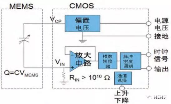
When the MEMS microphone works normally, a very stable DC bias voltage needs to be applied between the silicon-based sensitive diaphragm and the back plate made by the MEMS process to convert the capacitance change between the diaphragm and the back plate caused by the sound pressure into The weak electrical signal is amplified and output by the amplifier circuit of the ASIC chip. The ASIC chip design of the MEMS microphone includes the design of the bias voltage circuit, the design of the operational amplifier circuit, the design of anti-static protection, and the power supply voltage detection circuit. If the bias voltage provided by the ASIC is abnormal, it will cause a lot of extra noise after the weak electrical signal on the MEMS is amplified, which will seriously affect the acoustic performance of the MEMS microphone. If the design of the amplifying circuit is unreasonable, the electrical signal generated by the MEMS sensitive diaphragm cannot be extracted. FIG. 1 is a schematic diagram of an equivalent circuit of a MEMS digital microphone. Driven by the pursuit of low power consumption and small size, how to achieve high bias voltage stability and reduce the area of ​​ASIC chips is a problem that must be considered and solved.

Figure 1 Schematic diagram of the equivalent circuit of a MEMS digital microphone
There are many main performance parameters of MEMS microphones. This article mainly focuses on the three parameters of sensitivity, noise and signal-to-noise ratio. Sensitivity refers to the electrical response of the output end to an acoustic input signal of 94dB sound pressure level (SPL) or a sine wave of 1kHz at a sound pressure of 1Pa, that is, the magnitude of the voltage Vs at the microphone output end under the action of a unit sound pressure. Noise refers to removing the input signal when testing the sensitivity, and measuring the voltage Vn at the output terminal at this time. Because the values ​​of the voltages Vs and Vn are relatively small, the industry usually adopts the dB counting method. The signal-to-noise ratio value is 20Log(Vs/Vn). It can be seen that noise is an important performance indicator of MEMS microphones, which directly affects the size of the signal-to-noise ratio. There are two main sources of noise in the application process of MEMS microphones: one is the mechanical vibration noise of the MEMS chip itself, mainly because the MEMS chip is directly connected to the outside world through the sound through hole, which is obviously disturbed by the external environment. The second is the electrical noise of the ASIC chip itself. Due to the complex structure of the ASIC chip itself, it contains a large number of electronic devices, which mainly include the equivalent output noise of the bias circuit and the equivalent input noise of the readout circuit.
3 MEMS microphone noise failure analysis method
For the failure of MEMS microphone noise, the first task is how to quickly determine the specific source of the noise in a non-destructive manner. To this end, the author breaks the conventional test method and creatively adopts the test sample noise in the vacuum chamber. The advantage of this method is that the mechanical noise caused by the vibration of the MEMS chip can be eliminated to the greatest extent. By comparing the test results with the normal sample, if the test noise is high According to the normal test results, the noise source is mainly from the electrical noise of the ASIC chip; if the test value is equal to the normal value, the noise source is mainly the vibration noise of the MEMS chip. Once the specific failure location is determined, it is easier to find the failure cause through a series of electrical performance failure location and physical failure analysis methods.
Usually, for the specific case of MEMS microphone noise failure analysis, most of them are abnormal electrical noise caused by ASIC chip manufacturing process defects. The analysis points mainly focus on the following parts: 1) Whether the bias voltage is within the specification range; 2) The static and dynamic operating currents are within the specification range; 3) Whether the leakage current is abnormal; 4) Whether the micro-signal amplification process is normal, this process often generates a small signal through the signal generator to simulate the output of the MEMS, and then verify whether the ASIC works normally; 5) For digital MEMS microphones, also analyze whether the clock signal channel and channel selection are abnormal.
4 Case study
4.1 MEMS microphone electrical performance test results
Under the working voltage of Vdd = 2.75V, the test results of abnormal samples #1 and #2 are shown in Table 1:

The test specification of the MEMS microphone: 38 ± 3dB, it can be seen that the sensitivity is within the normal range, and the noise value is obviously high, resulting in a signal-to-noise ratio far below its specification value.
Figure 2 Noise (A-weighted) test spectrum of sample #1
4.2 Noise spectrum of failed samples tested in vacuum chamber
The noise sources of MEMS microphones mainly include the mechanical vibration noise generated by the vibration of the MEMS chip and the electrical noise of the ASIC chip. Therefore, before the destructive analysis, it is necessary to determine which part of the noise failure mainly comes from, so as to further analyze the specific failure. reason.
In this paper, the noise spectrum of the MEMS microphone tested in the vacuum cavity is used, and the main purpose is to eliminate the interference of the mechanical vibration of the MEMS. By comparing with the normal sample, it is found that the noise spectrum curve of the failed sample is obviously high, and it is preliminarily determined that the noise is mainly from electrical noise. , it is necessary to further confirm whether the relevant electrical performance parameters of the ASIC chip are normal.
Figure 3 Noise spectra of samples #1, #2 and normal samples in a vacuum chamber (without A-weighting)
4.3 ASIC chip-level electrical noise measurement
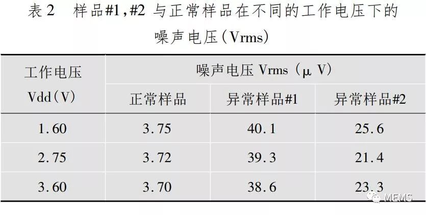
Through the physical destructive method, the MEMS microphone chip package shell is separated, and the electrical signal connection between the ASIC chip and the MEMS sensor is disconnected, and the electrical noise voltage (Vrms) of the ASIC chip test output is directly measured. The test results are shown in Table 2. .

Through the physical destructive method, the MEMS microphone chip package shell is separated, and the electrical signal connection between the ASIC chip and the MEMS sensor is disconnected, and the electrical noise voltage (Vrms) of the ASIC chip test output is directly measured. The test results are shown in Table 2. .
4.4 ASIC chip bias measurement
Under the same reference voltage inside the ASIC bias circuit, the bias voltage of the normal and abnormal samples is compared by testing, and it is found that the bias voltage of the abnormal sample is about 1V lower than that of the normal sample. Therefore, it is necessary to further determine the cause of the abnormality in the bias voltage region.
Figure 4. Relationship between ASIC chip reference voltage and bias voltage
After Vdd is powered off, within the same time interval, the test found that the bias voltage of the abnormal sample decreased significantly faster than that of the normal sample. The results are shown in Figure 5. Therefore, it is suspected that there is a possibility of leakage current in abnormal samples.
Fig. 5 The relationship between the power-off time of the working voltage and the bias voltage
4.5 Leakage current measurement of ASIC chip
By comparing the leakage current of the normal sample and the abnormal sample, it is found that the leakage current of the abnormal sample has obvious leakage current in the normal bias voltage range (34~36.5V), which is 4~6nA larger than that of the normal sample. See Image 6.
Figure 6 Leakage current test results of normal samples
Figure 7 Leakage current test results of abnormal samples
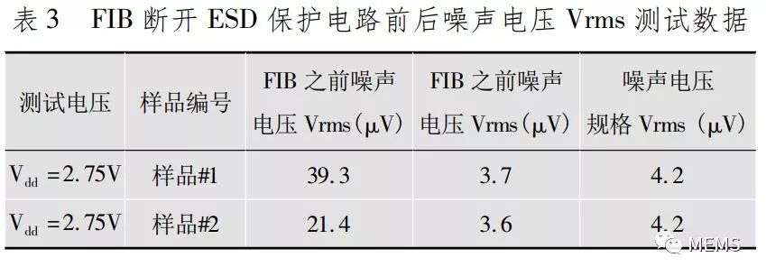
Based on the design of the ASIC chip, it is suspected that the leakage current channel exists inside the ESD protection circuit of the bias voltage. Disconnect the ESD protection circuit through FIB, and re-test the noise voltage Vrms of samples #1 and #2 under the working voltage of Vdd = 2.75V. The test results are shown in Table 3.

It can be seen from the test results that after the FIB disconnects the ESD protection circuit, the noise voltage Vrms of the failed samples #1 and #2 are both lower than the test specification value, indicating that the high noise voltage is mainly caused by the high leakage current of the ESD protection circuit. .
4.6 Failure Location and Physical Failure Analysis
Silicon-controlled rectifier SCR has high ESD protection capability per unit layout area. Using this special device, the ESD protection capability of the ASIC chip can be effectively and greatly improved in a small layout area without requiring additional processing in the process. Based on the relevant information of ASIC design, the ESD protection circuit of this chip is mainly realized by SCR. By locating the OBIRCH electrical performance failure of the ASIC chip, it is found that the ESD protection circuit area is obviously abnormal. According to the ASIC layout, it can be judged that the abnormal area is located on one side of the thyristor SCR, while the other side is normal, as shown in Figure 8.
Figure 8 OBIRCH shows the failure area on the SCR side
It can be seen from the SCR layout of the ASIC chip in Figure 9 that the horizontal physical distance between the Poly and Diffusion layers is designed to be 180 nm.
Figure 9 SCR layout of ASIC chip
The local cross-sectional analysis of the OBIRCH anomalous area by FIB can be seen from Figure 10: the distance between Poly and Diffusion on the left side of the SCR is 294.3nm, and the distance on the right side is only 67.50nm. From this, it can be judged that there is an obvious offset in the Poly layer, which leads to a significant difference in the physical distance between the Poly and Diffusion on the left and right sides. Since the spacing on the right side is only 67.50nm, it is very easy to cause leakage current when the ASIC works normally, which is consistent with the location of OBIRCH electrical performance failure, and also proves that the aforementioned assumption that leakage current causes noise failure is true.
Figure 10 FIB diagram of Poly and diffusion on the left and right sides of SCR
4.7 Improvement measures
In order to solve the problem that the physical distance between the poly and diffusion layers of the ASIC chip is too small, the slight offset in the process will lead to the existence of leakage current and affect the noise performance of the MEMS microphone. The physical distance between the two has been further optimized and adjusted. Appropriately increase the horizontal physical spacing on the original basis. The specific data are shown in Figure 11 and Figure 12. After mass production of 1 million MEMS microphones, there is no defective product with noise failure.
Figure 11 Layout of the improved SCR
Figure 12 The improved layout of SCR
5 Conclusion
This paper analyzes a specific case of MEMS microphone noise failure, and verifies the feasibility of measuring noise in a vacuum cavity to quickly locate the noise source. By comparing the noise values ​​of the failed samples and normal samples, it is possible to quickly locate the noise failure mainly caused by the electrical noise of the ASIC chip. For ASIC chip-level electrical failure location (OBIRCH) and physical failure analysis (FIB, SEM), the failure reason is mainly due to the serious offset of the position of the Poly and Diffusion layers in the ASIC chip manufacturing process, resulting in leakage current in the protection circuit area of ​​the bias circuit. road. The physical distance between the two was further optimized and adjusted, and the physical distance was appropriately increased on the original basis to completely solve the recurrence of such problems.
Sapphire glass. Similar to corundum, it has a hardness of 9. It can produce various colors by adding various chemical elements. The commonly used ones are colorless. It has the advantages of higher hardness and higher price than ordinary glass. It is mainly used to make high-end watch mirrors.
Germanium sapphire glass has good thermal properties, excellent electrical and dielectric properties, and is resistant to chemical corrosion. It has high temperature resistance, good thermal conductivity, high hardness, infrared penetration, and good chemical stability. Therefore, it is often used to replace other optical materials to make optical components, infrared-transmitting optical windows, and is widely used in infrared and far-infrared military equipment, such as: used in night vision infrared and far-infrared sights, night vision cameras and other instruments And satellite and space technology instruments and meters, as well as windows for high-power lasers, various optical prisms, optical windows, UV and IR windows and lenses, observation ports for low-temperature experiments, and high-precision instruments for navigation, aerospace, and aviation. Be fully applied.
For example, infrared transparent window materials, substrate substrates in the field of microelectronics, laser substrates, optical components and other applications.
Sapphire Lens,Sapphire Prism,Crystals Germanium,Germanium Lens Prism Window,BaF2Lens Prism Window
Bohr Optics Co.,Ltd , https://www.bohr-optics.com