In many applications, such as servers, the load transient response requirements of power rails are becoming more stringent. In addition, loop compensation design is often seen as a difficult and time consuming task for many engineers due to the complex Laplace transform function calculations involved.
This article will first discuss the average small-signal mathematical modeling of the widely used peak current mode (PCM) continuous current (CCM) DC-DC converter. It was then simulated using ADI's switching circuit simulation tool, ADIsimPE/SIMPLIS, to minimize complex computational effort. Subsequently, a simplified model was inferred for simpler, faster loop compensation design and simulation. Finally, we used the ADP2386EVAL evaluation board for loop testing. The results show that the loop crossover frequency, phase margin, and load transient response simulation results are well matched with the test results.
PCM average small signal modeling
As shown in Figure 1, the current mode DC-DC converter consists of six modules: feedback resistor divider, compensation network, current sense and sampling, comparator, power stage, and output network. In the loop, the inductor current ramp signal is compared to the compensated output voltage error signal to generate a PWM signal to drive the switch to modulate the inductor current. The inductor current flows into the output capacitor and load. Among all six modules, the power stage is the only nonlinear module and the most difficult module for DC-DC modeling.
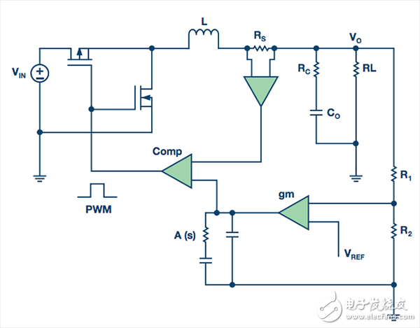
Figure 1. Block diagram of a current-controlled buck converter.
Model the power level with a 3-terminal switch:
l Active switch end (A)
l public (C)
l Passive switch (P), as shown in Figure 2, we can get the following formula 1:
iIN = iLd, VPC = vINd (1)
DC-DC converter modeling and loop compensation design considerations for peak current mode and continuous current mode
This is a transformer that is equivalent to a three-terminal switch with a turns ratio of 1:d, which is an average model that is only effective in continuous current mode. Deriving it to get the formula 2:
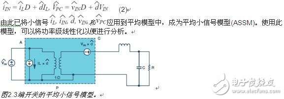
Taking the PCM CCM buck converter as an example, it is modeled by Laplace, and the block diagram is shown in Figure 3. There are two control loops: voltage loop and current loop. In the current loop, the inductor current signal detected by the RT is sampled as the first negative input signal to the comparator. In the voltage loop, the output voltage ripple is detected by the resistor divider of gain K as the positive input of the comparator after the compensator network Av(s). The inputs of the two loops are compared with the slope compensation signal to generate a duty cycle signal that drives the power level of the average small signal model to modulate the inductor current.
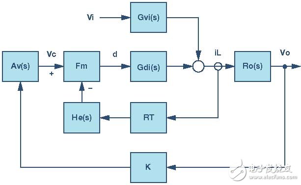
Figure 3. Block diagram of the PCM CCM DC-DC control model.
The gain function from the inductor current to the output voltage is the output load network function as shown in Equation 3:
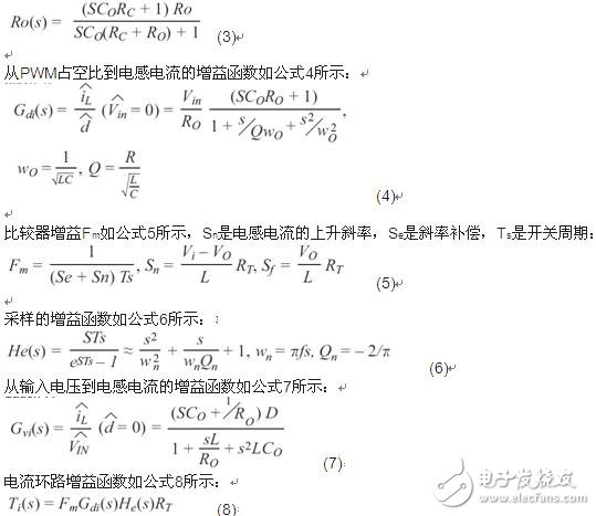
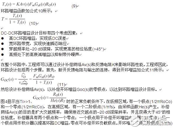
The voltage loop gain function is shown in Equation 9:
Conducive to noise suppression.
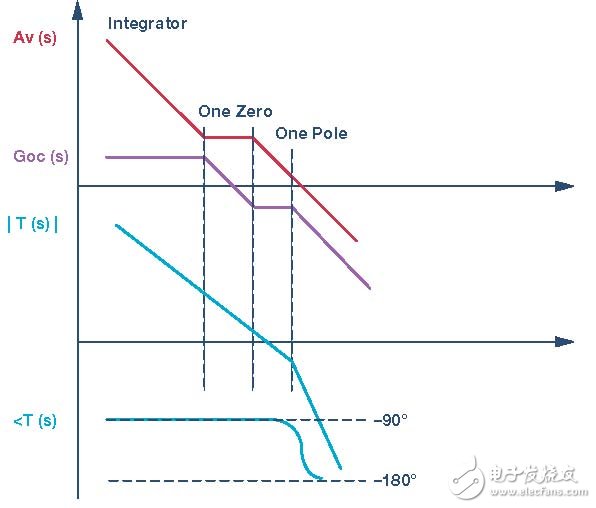
Figure 4. PCM CCM DC-DC loop design steps.
The ADsimPE tool with SIMetrix/SIMPLIS is a personal version of the circuit simulation software that is ideal for evaluating linear and switching devices from Analog Devices. SIMetrix is ​​suitable for linear circuits such as operational amplifiers, and SIMPLIS is for various switching devices such as DC-DC converters and PLLs. In Figure 5, a PCM CCM buck converter reference circuit is built to check circuit behavior and ASSM model accuracy. This is a PCM synchronous step-down transformer with a 3.3 V input, a 1.2 V output, and a 1.2 MHz switching frequency.
The calculation and simulation results are shown in Fig. 6. In the loop gain calculation result of the average small signal model on the left side, the crossover frequency is 50 kHz and the phase margin is 90.35°. The SIMPLIS simulation results can be seen on the right side of Figure 6, with a phase margin of 90.8° at a crossover frequency of 47.6 kHz. This proves that the ADIsimPE/SIMPLIS switching circuit simulation results are consistent with the complex ASSM calculations, which provide designers with a fast loop design approach. However, the schematic construction shown in Figure 5 is not straightforward.
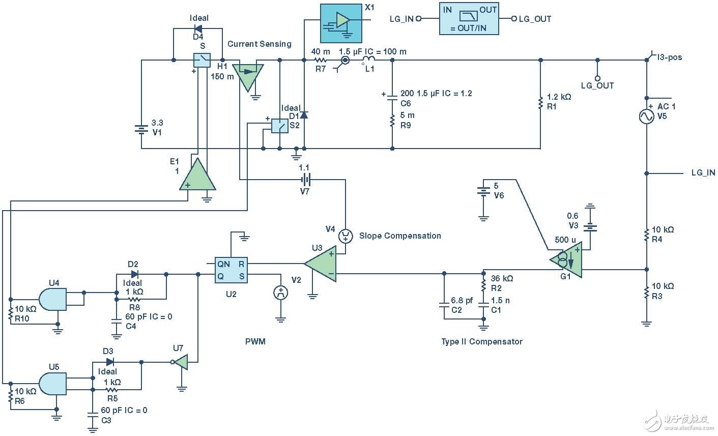
Figure 5. SIMPLIS reference circuit for PCM CCM buck converter.
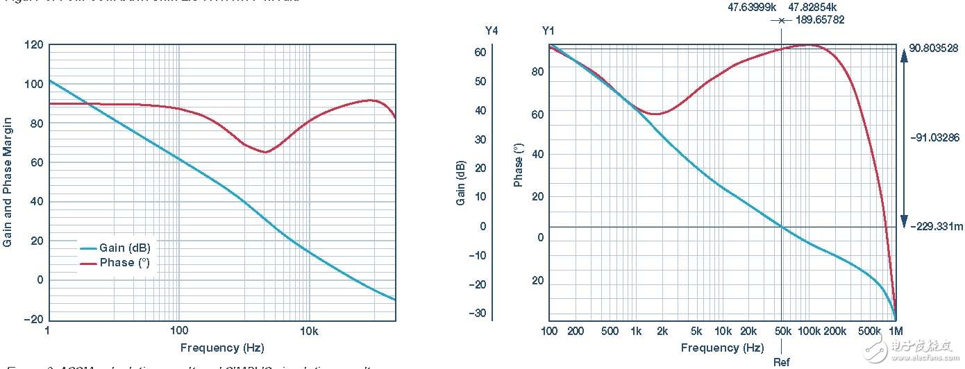
Figure 6. ASSM calculation results and SIMPLIS simulation results.
PCM simplified average small signal modeling
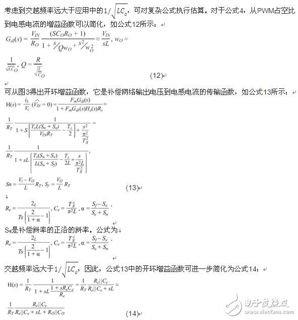
This means that the open-loop ASSM can be simplified to the current source controlled by the compensator output voltage, flowing into the RLC network that produces the inductor current, as shown in Figure 7. This model for simulation or calculation is much simpler than the original complex formula.
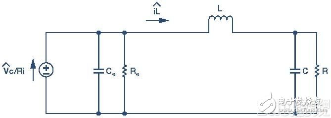
Figure 7. Simplified ASSM open-loop circuit.
Using the reference circuit in Figure 5, calculate Re and Ce, and then establish a closed-loop simplified ASSM circuit in ADSimPE, as shown in Figure 8. The SIMetrix simulation results are shown in the right half of Figure 8. The crossover frequency is 49 kHz and the phase margin is 90.5°, which matches the ASSM calculations shown in Section 2 and the SIMPLIS simulation results.
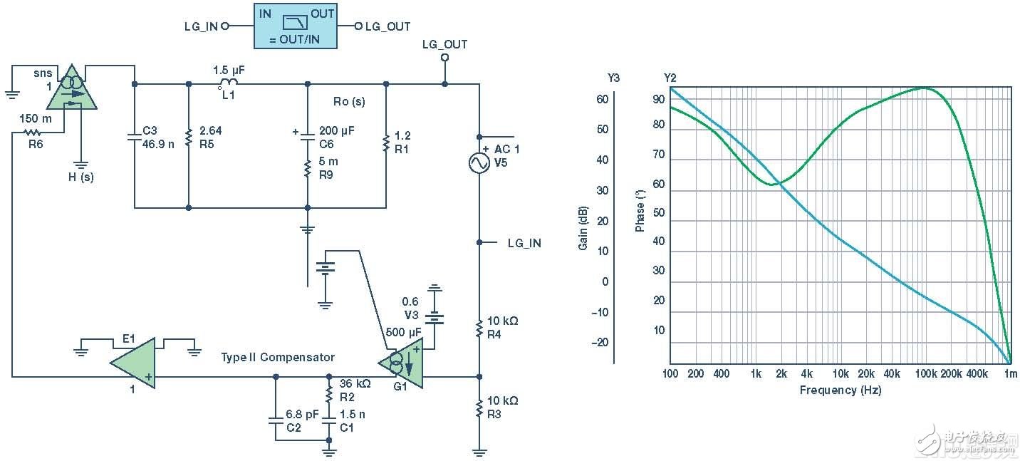
Figure 8. Simplified ASSM simulation circuit and results.
ADP2386 modeling simulation and test results
The ADP2386 is a synchronous PCM CCM step-down transformer from Analog Devices. It supports input voltages up to 20 V and output voltages as low as 0.6 V with output currents up to 6 A and switching frequencies between 200 kHz and 1.2 MHz. The versatility of the device allows it to be used in buck applications and inverting Buck-Boost topologies without increasing cost and size. In this section, the model test results are validated using the loop test and load transient test results of the ADP2386EVAL evaluation board.
The schematic of the ADP2386EVAL is shown in Figure 9. For testing purposes, we set up the EV kit according to the conditions shown in row 1 of Table 1 below. The abbreviated relationship between the internal slope compensation of the ADP2386 and the duty cycle is that we use Equation 14 to obtain the simplified ASSM parameters, as shown in the second row of Table 1. The output capacitor's capacitance is reduced by approximately 30% at 3.3 V, so in a simplified ASSM simulation, the output capacitor value has been changed to 100 μF instead of 147 μF in the evaluation board.
Table 1. ADP2386EVAL test conditions and simplified ASSM parameters
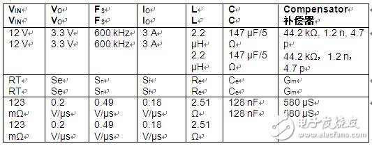
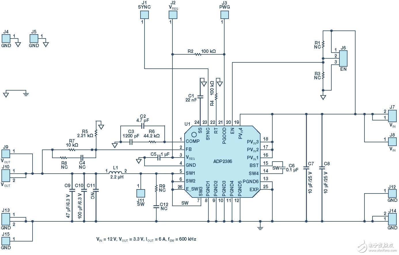
Figure 9. ADP2386EVAL schematic.
Figure 10 shows the simplified ASSM simulation and actual test results for the ADP2386EVAL loop. On the left is the simulation of ADIsimPD/SIMetrix – the crossover frequency is 57 kHz and the phase margin is 71°. On the right is the AP Model 300 test result – the crossover frequency is 68.7 kHz and the phase margin is 59.3°. Although there is a difference between the test results and the model simulation, we can know from the data sheet of the ADP2386 that its error amplifier gain varies from 380 μS to 580 μS, and there are errors in the inductance and output capacitance. Therefore, the difference between the two results is acceptable.
The load transient test consists of two tests. Test 1 was tested under the compensator conditions shown in Table 1, with good phase margin and wide crossover frequency. In Test 2, the compensator was changed to 100 pF/1.2 nF/44.2 kΩ, the crossover frequency dropped to 39 kHz, and the phase margin dropped to 36°. Figure 11 shows the test transients and test results for load transients (0.5 A to 3 A, 0.2 A/μs). In the actual test, the overshoot peak was 67 mV, the simulation result was 59 mV, and the transient curve was also well matched. Figure 12 shows the load transient (0.5 A to 3 A, 0.2 A/μs) test 2 simulation and test results. In test 2, the overshoot peak was 109 mV, the simulation result was 86 mV, and the transient curve also matched well.
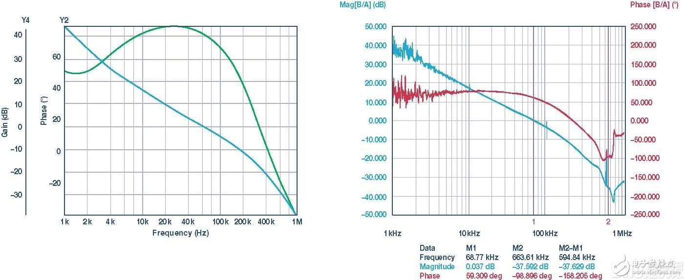
Figure 10. ADP2386EVAL loop simulation and test results.

Figure 11. ADP2386EVAL Load Transient Test 1 Simulation and Test Results.

Figure 12. ADP2386EVAL Load Transient Test 2 Simulation and Test Results.
in conclusion
Loop compensation is often seen by engineers as a very challenging design task, especially in fast load transient applications. Based on the widely used peak current mode continuous current buck device, this paper briefly summarizes the average small signal mathematical modeling and loop calculation, as well as the simpler ADISimPE/Simplis simulation. This article also introduces a simplified average small-signal model and provides a simplified method for processing loop compensation designs. The ADP2386EVAL evaluation board loop and load transient test bench test results demonstrate the accuracy of the simplified model and its simulation.
Tianma Microelectronics Co.,Ltd., founded in 1983, is a high-tech enterprise specializing in the production and operation of liquid crystal display (LCD) and liquid crystal display module (LCM). After more than 30 years of development, has developed into a set of LCD research and development, design, production, sales and service as one of the large public listed companies. Tianma of Shenzhen, Tianma of Shanghai, Tianma of Chengdu, Tianma of Wuhan, Tianma of Xiamen, Tianma of Europe, Tianma of the United States, Tianma of South Korea, etc. STN-LCD, CSTN-LCD, TFT-LCD and CF production lines and module factories. The company's marketing network throughout the world, products are widely used in mobile phones, MP3/MP4, on-board display, instrumentation, household appliances and other fields. In terms of technical level, product quality, product grade and market share, it ranks among the top in the same industry in China and has become a leading enterprise in the field of small and medium-sized display.
The company is mainly engaged in the design, manufacture and sales of LCD and related materials, equipment and products, providing related technology development, technical consultation, technical services and technology transfer, and engaged in the import and export of goods and technology. Specializing in LCD screen and module design, research and development, manufacturing, sales and after-sales service. Production used for LCD, laptop, LCD TV, digital video and audio, car GPS, industrial medical products and other models of display screen and module. Products are widely used in mobile terminals, car display, aviation display, industrial control medical, entertainment display and other small and medium-sized display fields.
Tianma TFT-LCD,Nextion 3.5,Arduino Tft Screen,Raspberry Pi 3.5 Lcd,3.5 Inch Raspberry Pi Screen
TONYA DISPLAY LIMITED , https://www.tydisplay.com