This article is mainly about the introduction of Samsung 788DF, and focuses on the principle of video processing of Samsung 788DF and the principle of display circuit in detail.
Samsung 788DF video processing circuit diagram detailedThe video processing circuit of this machine is composed of RGB three-primary color signal preamplifier circuit IC102 (NT6813), RGB three-primary color signal output amplifier circuit IC106 (STV9588), and CRT auxiliary circuits as the core components, as shown in Figure 11-9.
1. Pre-amplification circuit
The pre-amplification circuit is composed of IC102 (NT6813) as the core, and the pin functions of NT6813 are shown in Table 11-4.
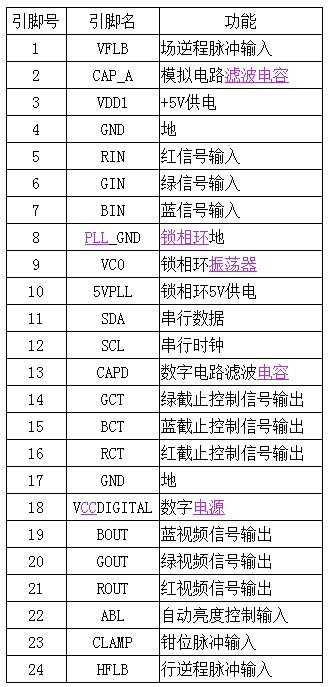
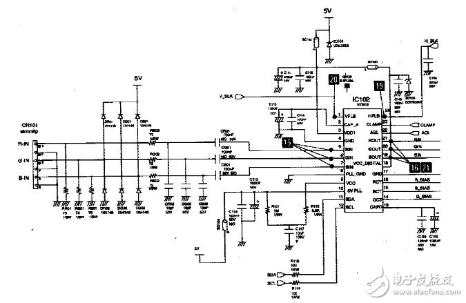
The R, G, and B three-way analog signals output by the computer host are input to the video signal processing circuit board through the connector. Among them, the R primary color signal is sent to the 5 pin of the NT6813 through RR02 and CR01, and the G signal is sent to the NT6813 through the RG02 and CG01. At pin 6, the B signal is sent to pin 7 of NT6813 via RB02 and CB01. After being amplified by NT6813, the R, G, and B signals are output from 21, 20, and 19 pins.
The 23 pin of NT6813 is the clamp pulse input terminal. Under the action of the clamp pulse, the video clamp circuit is in working state, so that the 21 pin, 20 pin, and 19 pin of NT6813 have video signal output. If the NT6813 has no clamp pulse voltage input, the R, G, and B amplifiers of the NT6813 will be cut off, and the picture tube will be black.
2. Video output circuit
The video output circuit is composed of IC106 (STV9588) as the core. STV9588 pin functions are shown in Table 11-5.
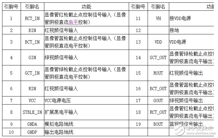
The R, G, and B signals output from the 21, 20, and 19 pins of the NT6813 are added to the 6, 4, and 2 pins of the STV9588 respectively. After being amplified by the STV9588, the R, G, and B primary color signals are output from the 15, 17, and 19 pins respectively. It is coupled to the three cathodes of RK, GK and BK of the picture tube via CR04, CG04 and CB04.
LR01, LG01, LB01 are used to improve the high-frequency quality of the picture. DR05, DR03, DG05, DG03, DB05, DG03 are set to prevent the STV9588 from sparking and damaging the picture tube. SKR01, SKG01, and SKB01 are electric dischargers, and their function is to prevent the damage caused by the ignition of the picture tube.
3. White balance adjustment circuit
1. Dark balance adjustment The dark balance adjustment is to adjust the static working voltage of the picture tube RK, GK, BK, so that the cut-off points of the three electron beams are moved to the same position to ensure that the screen does not cast color at low brightness.
When the cathode potential of the kinescope RK needs to be changed, the microprocessor IC201 changes the DC voltage output by the 16-pin of the NT6813 through the I2C bus. After processing by IC106 (STV9588), it controls the 18-pin DC potential of the STV9588 to change, thereby controlling the CRT's RK cathode potential. The adjustment process of the cathode potential of GK and BK is no longer analyzed.
2. Bright balance adjustment Bright balance is achieved by changing the gain (signal amplitude) of the R, G, and B primary color signals to ensure that the picture does not cast color at high brightness.
When the R signal gain needs to be changed, the microprocessor IC201 controls the NT6813's R channel amplifier signal gain to change through the II2C bus, and then controls the NT6813's 21 pin output to change the R signal amplitude. The adjustment process of G and B signal gain is no longer analyzed.
Four, contrast and ABL control circuit
1. Contrast control circuit Contrast is achieved by controlling the gain of the three primary color signals of R, G, and B. When it is necessary to increase the contrast, the microprocessor IC201 controls the gain of the R, G, B three-channel amplifiers of the NT6813 through the I2C bus to increase, so that the picture contrast can be increased.
When reducing the contrast, the control process is reversed.
2. ABL control circuit. When the brightness of the picture increases and the current of the picture tube bundle increases, the voltage of pin 8 of the line output transformer T501 drops, which causes the voltage of pin 22 of NT6813 to drop, and controls the gain of the internal R, G, B amplifiers to decrease, so that the picture tube The beam current is reduced to avoid the harm caused by excessive beam current.
Five, brightness control and elimination of bright spots circuit
1. Brightness control circuit
The brightness control circuit of this machine does not adopt the common grid control method, but adopts the cathode control method.
The video amplifier output adopts AC output mode. The video amplifier output is a clamped video signal. Therefore, the brightness of the grating depends on the DC level (black level) of the cathode of the kinescope. The brightness control circuit is controlled by the microprocessor IC201 through the IIC bus. The signal processing circuit NT6813 is completed. When the brightness needs to be adjusted, the DC voltage output by the 21, 20, and 19 pins of the NT6813 will change at the same time. After the STV9588 is processed, the DC voltage output by the 18, 14 and 16 pins of the STV9588 will be changed at the same time, and then the DC voltage of the cathode of the kinescope will be controlled. The brightness of the grating changes to achieve the purpose of brightness control.
2. Eliminate the bright spot circuit
The negative pulse voltage on the 9th pin of the secondary winding of the line output transformer T501 is rectified and filtered by D504 and C505 to obtain a negative voltage of -150V. When the display is working, the transistor Q512 is always on because the emitter voltage is always higher than the base voltage, so the -150V voltage is divided by R514, R515, Q512 and then applied to the grid G1 of the picture tube, which is The picture tube grid provides the negative pressure required for normal operation. After the display is turned off, Q512 cuts off quickly, and the -150V voltage is directly applied to the picture tube grid G1 without being divided by Q512. Because of this large negative pressure, the electron beam can be cut off and the shutdown bright spot is eliminated.
Six, line and field blanking circuit
1. Line blanking circuit
The line blanking is not applied to the grid of the kinescope, but the line retrace pulse from the line scan output circuit is applied to the video signal processing circuit NT6813 to complete the line blanking. The specific working process is: the line retrace pulse generated by the line scan circuit is added to the 24 feet of the NT6813. The scan can be blanked during the reverse travel period to avoid retrace lines appearing on the phosphor screen.
2. Field blanking circuit
Field output integrated circuit IC301 (STV9325) of the 3-pin output field flyback pulse V-BLK, C307, R311 added to the base of Q512, Q512 inverted and output from the collector, during the vertical blanking period, it is added to The voltage drop (more negative) of the G1 pole of the picture tube reduces the brightness of the screen scene and achieves the purpose of eliminating the field retrace line.
Seven, video squelch circuit
At the moment of power-on or mode change, the 8-pin of the microprocessor IC201 outputs a short high level, controls Q511 to turn on, and Q512 to turn off, so that the negative pressure on the G1 pole reaches the negative maximum value, and the grating on the phosphor screen disappears. Video squelch.
The display is the most basic output device. The use of the display is the most basic way to observe the display of characters and the information of the image more conveniently. The processing method on the computer is parallel digital signals, and the display processing is serial analog. Signal, so the received digital signal is processed on the display card to form a TTL level signal or an analog signal. The display system also includes a display card and a display.
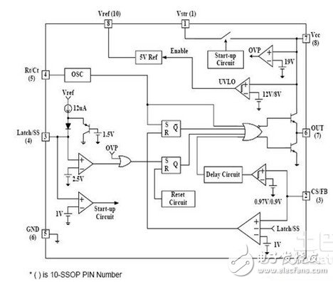
Understanding the composition of the display circuit diagram is of great help to maintenance and repair, and the understanding of the display circuit diagram can also clarify the composition information of the display circuit diagram, and can also fully penetrate the function of the display.
The composition of the display circuit diagram
First of all, the circuit diagram of the display is composed of image high and intermediate frequency circuit, chromaticity circuit, brightness circuit, synchronization separation circuit, line scanning circuit, field scanning circuit, power supply circuit and picture tube, and a blood auxiliary circuit. Among them, in the composition of the image high-intermediate frequency circuit, the involved parts include a high-frequency head, an intermediate frequency amplifier, and a video detector. The components involved in the sound circuit include the sound amplifier, the frequency discriminator, and the local amplifier. The horizontal scanning circuit manages the phase detector and the horizontal oscillator, as well as the horizontal excitation, horizontal output, and medium and high voltage circuits. The scanning circuit dominates the field oscillator, as well as the sawtooth wave forming circuit, as well as the field excitation and field output.
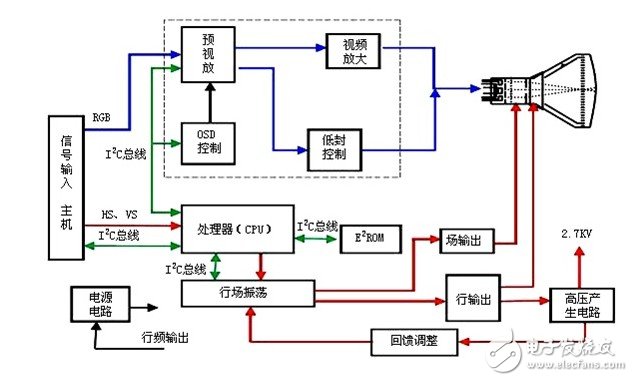
In a simple point, from the management level, the display circuit diagram mainly consists of a power supply circuit and a system common governance circuit, as well as a line and field scanning circuit, and the video RGB analog three-primary color signal circuit is composed.
Display circuit diagram circuit introduction
First of all, let’s talk about the most important power supply circuit in the display circuit diagram. First, the power supply circuit is composed of the main power supply, which is the primary power supply, as well as the line output power supply and the energy saving circuit. The principle of the main power supply and the switching power supply are very similar, the main thing is to provide the power supply voltage of the whole circuit of the display.
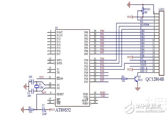
The horizontal scanning circuit will change due to the change of the horizontal oscillation frequency of the multi-frequency numerical control color display. In the horizontal scanning circuit, there is an automatic S correction capacitor switching circuit, a reverse capacitor switching circuit and an automatic linear inductance adjustment circuit, etc. Composed together.
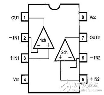
Regarding the display circuit diagram is very complicated, different circuit management has different display devices, and the composition of the display circuit diagram is from the main circuit to the auxiliary circuit to the line scanning circuit and the field scanning circuit. It is indispensable and must be fully maintained If you understand what circuit and what equipment to manage, it will be easy to maintain.
ConclusionThis is the end of the related introduction about Samsung 788DF. Please correct me if there are any deficiencies.
Related Reading Recommendations: Encyclopedia of Display High Voltage Bar Circuit Diagrams Related Reading Recommendations: How to deal with LCD flickerZhejiang Synmot Electrical Technology Co., Ltd , https://www.synmot-electrical.com