A few years ago, when I was working at Teradyne, the leader in automatic test equipment (ATE), I often encountered a fundamental dilemma: in the production/test shop, it was better to pass an unqualified device, or to eliminate one piece. Is the qualified device better? Obviously, these two are not good choices. If you remove a qualified device, it will result in a decline in your manufacturer's output, a decline in profits, and subsequent losses. However, if you pass an unqualified device, undetected manufacturing defects will eventually be demonstrated in the actual application phase, at which point the cost of repairing the defect will be several times higher than the cost of the manufacturing floor. , thereby affecting profits, and more serious is affecting customer reputation.
These are still applicable today, and they are even worse. Recent statistics indicate that the cost of testing a chip for manufacturing defects (compared to the absence of design defects) has increased to 40% of manufacturing cost after fabrication.
Many of these factors have driven the electronics industry to find ways to put testability into the chip at the design stage, thereby reducing test costs. This method is called Testability Design (DFT) and has the following effects:
Ensure that all faults in the circuit are detected
Reduce the cost and time associated with test development
Reduce the execution time required to test and manufacture chips
Overall, over time, two forms of DFT have emerged in the industry: ad-hoc DFT and structured DFT.
Ad-hoc DFT includes a set of rules that promote "good" design specifications designed to simplify and speed up the testing process. For example, provide set and reset signals so that all flip-flops can be initialized; avoid asynchronous logic feedback that causes oscillations; logic gate design should take care to avoid excessive fan-in numbers (fan-numbers are too large to cause observable inputs and control outputs) Or provide test control for signals that are difficult to control. For example, a signal generated by a long counter requires many clock cycles to control, which requires an increase in the length of the test sequence. In general, ad-hoc DFT does not add logic, ie does not consume silicon in the design.
Structured DFT: Scanning and BISTIn some processes, structured DFT will introduce additional test logic. The most common structuring methods are scanning and built-in self-testing (BIST).
In 1973, Williams and Angell first mentioned the word "scan". Sequential circuits are often difficult to test compared to combined designs. The main principle of the scanning method is to treat and observe the internal storage elements as part of a shift register chain for serial shifting. In the scan chain, the main problem with testing any circuit is to reduce the combinational logic between registers. The basic operation is to turn each flip-flop into a scan register. The only cost is the addition of a multiplexer. In normal mode, the trigger will operate in the normal way. In scan mode, the flip-flop will be used as a shift register. You can scan the contents of the output trigger or scan for new values. More importantly, this approach supports the development of automated test pattern generators (ATPGs) and reduces time-consuming and cumbersome test vector creation.
Over time, the complexity of the circuit has increased, and the cost of test program development is the same. The VLSI design of the 1990s and the SoC chip of the millennium have greatly increased the cost of test equipment and software development. Just consider:
The ultra-high and still increasing chip logic/pin ratio makes it more difficult to accurately control and observe the internal working conditions of the device, especially for testing.
SoC devices are getting denser and denser, and the voltage drop between process technology nodes is faster
Test pattern generation and application become extremely long
A large amount of test data must be stored in ATE
Full speed testing (GHz level) is getting harder and harder and the price is extremely expensive
Unfamiliar with the design of the design (DUT) gate level structure, because the logic of the hardware description language HDL is automatically synthesized, thus introducing testable insertion problems.
Professional test engineers are seriously lacking
In response to this unstoppable trend, the industry has integrated some of the tester's functions on the chip and named it BIST. BIST reduces complexity and in turn reduces costs and reduces reliance on external (programmed mode) test equipment in two ways:
Reduce test cycle duration
Reduces the complexity of test/probe settings by reducing the number of I/O signals that are driven/checked by the tester.
Then, BIST can implement a full-speed (GHZ-class) test circuit and then perform a more thorough inspection.
The basic approach is to compress the "good" test results (responses) into a "flag" and apply a pseudo-random (pseudo-exhaustive) pattern generator (PRG) to the chip. BIST essentially integrates pattern generation and response evaluation onto the chip.
In the most mainstream BIST method, when an input is applied to a logic module, the modified scan unit generates a pseudo-random test vector and then collects the output flag (via a linear feedback shift register). The BIST example includes an LFSR (Linear Feedback Shift Register) for generating a pseudo-random sequence and a MISR (Multiple Input Characteristics Register) for generating a measured circuit flag.
Although BIST occupies more silicon area and verification period (pseudo-random), it saves the cost of generating and storing test vectors. Moreover, because it often runs at full clock frequency, BIST typically takes up less time.
DFT verificationScanning and BIST design are usually incorporated into the design after the functional verification of the design is correct. Unfortunately, the insertion of an on-chip test architecture (ie, scan chain, BIST structure, and compression/decompression logic) can affect its own functional correctness. Therefore, gate level design verification must be performed after the DFT is implanted.
HDL simulation cannot do this right away. Given the complexity of the design, gate-level simulation can take several months (assuming several years) to complete a full and complete verification.
It can be said that the hardware simulation platform is tailored for this task.
Hardware simulation using the DFT App
Mentor Graphics recently released the DFT "App" for hardware emulation, which includes all the features needed to perform hardware accelerated emulation.
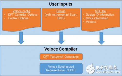
Its compiler creates the necessary test architecture to read test vectors from STIL files, then input these vectors into synthesizable DUTs and compare them for output. The compiler can also recompile user netlists into a structured description that is compatible with hardware emulation. See Figure 1.

With the DFT App, user input can be passed to the hardware accelerator's compiler. The hardware accelerator integrates the data of the DUT.

During operation, the Veloce hardware emulation platform extracts test vectors from the STIL file, applies them to the DUT, and compares the outputs at hardware emulation speed. .

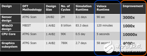
The hardware simulation execution speed is several orders of magnitude higher than the software simulation. According to the DFT App performance table summarized in the table, it can be seen that the running DFT mode is improved by four to five orders of magnitude. For software simulation tasks that take three months to complete, using hardware emulation can actually be done in just a few hours.
in conclusion
The DFT App implementation shortens the pattern development cycle by completing DFT verification mode settings in a reasonable amount of time. Scalable hardware and compilers support the effectiveness of larger gate-level scans and test structures embedded in the design. The DFT App supports standard STIL format files and works with other tools.
A hardware simulation process provides sufficient verification capabilities to ensure that DFT arrangements are completed within the timeframe of project management, thereby speeding time to market, increasing production, and ultimately increasing profits.
A solar carport is a canopy that captures solar energy placed over a parking area. They provide a huge opportunity to use otherwise wasted parking lot space to create renewable energy.
Solar carports offer a more efficient and unobtrusive way to gather energy from the sun when compared to ground-mounted systems. If space is an issue for your home or business, a solar carport is a great way to cash in on clean energy in the most efficient way possible.
Sunket in-house design/engineers and project managers emphasize the proposed site`s layout. Following our best practices allows the solar carport installer teams to value engineer our solar carports pre-engineered frames to best perform for the property and its owner, while also being economically efficient. A credible and experienced solar carport installer will tell you that no two parking lot properties are the same!
Solar Carport ,Solar Carport Structures, Solar Carports For Homes ,Solar Carport Kit ,Carport With Solar Panel , Roof Solar CarportsÂ
Wuxi Sunket New Energy Technology Co.,Ltd , https://www.sunketsolar.com