The OMAP5910 has a separate LCD control module inside, and its function is shown in Figure 1. It can be seen from the figure that the core unit of the LCD control module is the controller, which is responsible for the control of the other parts and the connection with the peripherals. The controller connects two peripherals, one for the DMA request to the OMAP5910 and one for the interrupt request to the peripheral's LCD. In this way, the 0MAP5910 is used as the master device, and the display core control of the LCD can be realized without the CPU participating. The LCD acts as a passive device, with a small amount of state that needs to be returned, sending an interrupt to the OMAP5910, and the OMAP5910 schedules the time to read the LCD state. In this way, the display and control of the entire LCD takes up less CPU resources.
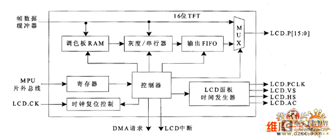
Figure 1 Functional block diagram of the LCD controller
The data channel of the LCD control module consists of three parts: palette RAM, grayscale/serializer and output FIFO. These three parts support the 12 or 16-bit STN mode, and the controller controls the output data to the data bus of the LCD. For the 16-bit thin film process (TFT, Thin ~ Film Technology), the data is directly transmitted to the LCD bus, providing 2 (16) = 64K color signals.
The register unit of the LCD control module is used to set the module. The register includes a control register, three time registers and a status register. Mainly used to set the width and height of the LCD, color or monochrome selection, passive or active display selection, pin polarity selection, frame clock pulse width, pixel clock and deflection frequency, and various status values. The controller can control and reset various clock signals according to the contents of the registers.
The control signals between the LCD control module and the TFT-LCD include four signals, PCLK (Pixel Clock Signal), HS (Horizontal Synchronization Signal), VS (Vertical Synchronization Signal), and AC (Output Enable Signal). The LCD control module outputs to the LCD.
The LCD driver circuit and the 0MAP5910 are connected as shown in Figure 2. Connect the LZ9FC22 using the OMAP5910's LCD controller interface. LZ9FC22 is a driver chip specially developed by Sharp to cooperate with LQ035Q7D LCD. It can be seamlessly connected with LQ035Q7D.
The LZ9FC22 is connected to the OMAP5910's LCD controller. Since the LZ9FC22 is an 18-bit controller (the RGB signals each have 6 bits), the output of the OMAP5910's LCD controller has only 16 bits of data. For this reason, two bits of data must be lost, and the RZ9FC22's R0 will be used. Ground with BO or connect R0 and R5, BO and B5 together.
The LCD's pixel sync clock signal, horizontal sync signal, vertical sync signal, and output enable are directly connected to the LZ9FC22. The LZ9FC22 has two horizontal and vertical refresh setting signals, HRVE and VRVE pins, which are controlled by two GPIO pins of the OMAP5910. The LCD refresh mode is set by changing the state of the GPIO pins. In order to ensure the normal operation of the LZ9FC22, the OMAP5910 provides a reset signal to the LZ9FC22. Once the LQ035Q7D displays abnormally or responds abnormally, the OMAP5910 controls the LZ9FC22 to return to the initial state through the reset pin.
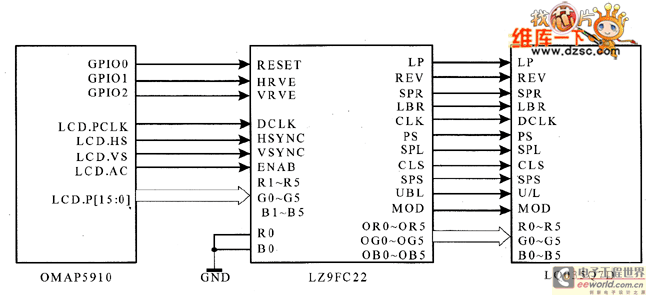
Figure 2 LCD drive circuit connection
The pin connections of the LZ9FC22 and 0MAP5910 are shown in the table.
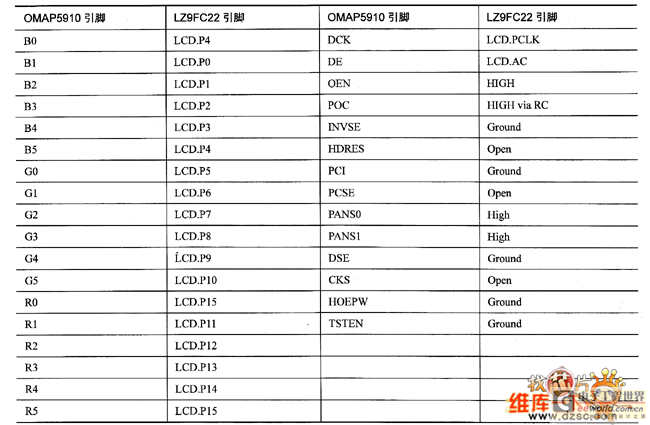
Table LZ9FC22 and OMAP5910 pin connection
The LQ035Q7D panel display requires a high voltage of 15V, while the logic level of the LQ035Q7D requires a 3.3V power supply. Figure 3 shows the principle of a power supply from 3.3V to 15V and 3.3V. Among them, 3.3V to 3.3V uses TI's TPS79333 to ensure stable and reliable output to LCD 3.3V. If the input 3.3V of TPS79333 is stable enough to meet the requirements of LQ035Q7D, it can also be directly connected to the LCD.
The backlight circuit of LQ035Q7D is shown in Figure 4. Use TI's TPS61042 to drive four LED tubes while using the PWM signal to control the voltage output to adjust the brightness of the four LED tubes. The PWM signal has a control frequency between 100 and 50 kHz. If the frequency is too low, flicker will occur. If you do not use the PWM signal, you can directly connect a GPIO pin and set the switch for high and low level control LEDs.
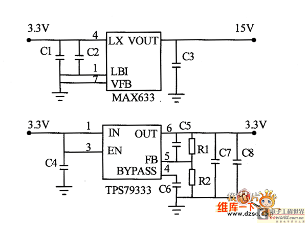
Figure 3 LCD power supply circuit design
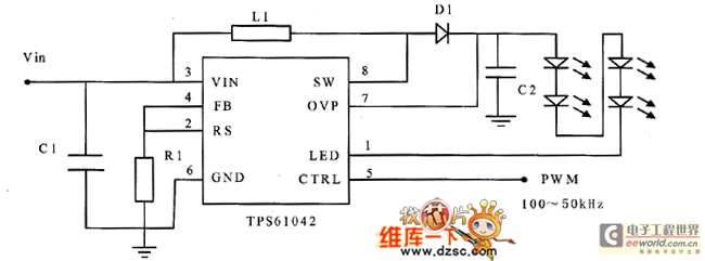
Figure 4 LCD backlight circuit design
The OMAP59 10 LCD driver software design includes four parts: touch screen drive, LCD drive, backlight drive, and LCD brightness drive. Among them, the LCD brightness is relatively simple to drive, set the OBL59l0 internal LCD Brt register to control the brightness of the LCD, the register is a 32-bit data format, set OxOFFFF FFFF for maximum brightness, OxOOOO OOOO for minimum brightness. In addition, the width of the yellow and red pixels of the output can be adjusted in the StLED-Gm and StLED-Red registers inside the OMAP5910 to change the brightness and color of the LCD.
The control of the LCD backlight is completed by the PWM signal of the OMAP5910. The PWT FRO register inside the OMAP5910 can be used to control the frequency of the output pulse. The PWT-VCR register inside the OMAP5910 can control the high level width of the output pulse, thus achieving backlighting. control.
Control of the LCD touch screen is done by the OMAP5910's Toucå»´Screen register. This register mainly sets the touch screen and the SPI interface protocol of the OMAP5910. Includes information such as touch interrupt response, SPI bidirectional data transfer, and SPI clock. In addition, you can also set the SPI CS chip select signal to turn the touch screen on or off. This function is very useful in systems where both the touch screen and the keyboard exist. When the OMAP5910 detects a keyboard interrupt, it can block the interruption of the touch screen, thus avoiding conflicts of multiple input information.
The design of driving LCD under Linux mainly includes frame buffer design, main structure definition, kernel configuration and compilation.
The frame buffer device provides an abstraction process for the image hardware device. It represents some of the video hardware settings, allowing applications to access image hardware through a well-defined interface. This software does not need to know anything about the underlying drivers of the hardware (such as hardware registers). It allows the upper application to directly read, write, and I/O control the display buffer in graphics mode. The device can be accessed through a dedicated device node, such as /dev/fb*.
In LCD controller operation, the frame buffer is used to store all coded pixel data for all screens. At its lowest address is a 32 or 512 byte buffer used to store the palette data table. A 32-bit buffer is used for a 16-item palette of 4, 12 or 16-bit pixel encoding; a 512-byte buffer is used to load a 256-element palette of 8-bit pixel encoding. In the case of 12 or 16-bit pixel encoding, the palette is not used, and the first 32 bytes of the frame buffer must be filled with all zeros.
USB4 Series Cable,USB 4 Cable,USB 4.0 Harness,USB Cable 4.0
Dong guan Sum Wai Electronic Co,. Ltd. , https://www.sw-cables.com