The use of IGBTs in any device will encounter IGBT selection and thermal design issues. After the two intuitive parameters of voltage stress and current stress are determined, the IGBT needs to be selected according to the loss and thermal cycle capability of the IGBT under the application conditions. Usually due to different operating conditions, the parameters given in the IGBT data sheet do not give an exact indication of the loss of the IGBT under the application conditions. A better method is to determine the difference between the measurement conditions of the parameters in the IGBT data sheet and the actual application environment through the measurement industry, and to introduce a simple measurement method for the loss of the IGBT.
Definition of IGBT parameters
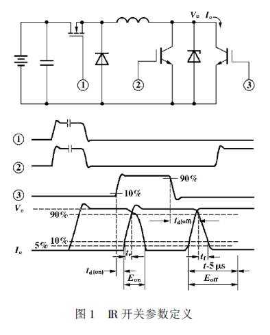
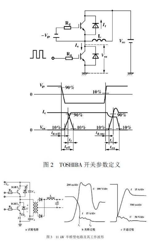
The IGBT switching parameters provided by the manufacturer are usually measured under purely inductive loads. Figures 1 and 2 are the circuits that measure the switching time of IR and TOSHIBA, respectively, and the waveforms that define the switching time. The common features are: Turn on the pure inductive load in the freewheeling state; Turn off the purely inductive load with the clamp diode. Some data sheets also show the energy loss of the switching process, which is also measured under the same conditions.
For a switching mode power supply that works in PWM mode and uses a transformer, its operation is quite different. Figure 3 shows an 11 kW half-bridge circuit and its operating waveform. The IGBT used is the GA75TS120U. As can be seen from the waveform, the current rise time tr is approximately 500 ns and the fall time tf is approximately 300 ns. However, in the data sheet, the current ramp time of the GA75TS120U is tr=100 ns and tf=80 ns, which is quite different from the actual working conditions. The reasons are mainly in the following two aspects:
(1) When opening, in Figure 3, due to the leakage inductance of the transformer, the IGBT actually turns on a zero-current inductive load, which is similar to zero current turn-on. The current rise rate is limited by the leakage-sensing charging speed, so the actual current rise time Tr does not depend entirely on the IGBT. In the data sheet, the pure inductive load in the freewheeling state is turned on. At the instant of turn-on, the IGBT must withstand the current in the inductor and also withstand the reverse recovery current of the freewheeling diode. The current rise rate is completely dependent on the turn-on of the IGBT. speed.
(2) When shutting down, the IGBT in Figure 3 is not shutting down one pure inductive load, but turning off one R - L type load (transformer and its load, which can be equivalent to R - from the primary side of the transformer) L-type load), its current fall time tf is slower than turning off the purely inductive load with clamp. Moreover, for a purely inductive load, the current of the IGBT begins to drop only after the collector voltage of the IGBT rises to the clamp value (see Figure 1, Figure 2), while the resistor-inductive load, the collector voltage and The current changes almost simultaneously (see Figure 3b waveform).
For the above reasons, the tr and tf of the IGBT in Figure 3 are both greater than the given value, but this does not mean the rise of the loss, because the switching loss also depends on the "overlap" of the voltage and current during the switching process, and in Figure 3 The "overlap" is obviously not as serious as in Figure 1 and Figure 2, so the overall loss will decrease.
IGBT loss measurement
The measurement of IGBT loss is actually obtained by measuring and calculating the operating voltage and current. Therefore, the measurement of loss is essentially the measurement of voltage and current. The appropriateness of the measurement method of voltage and current directly affects the measurement result. Credibility.
3.1 Current measurement
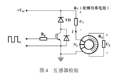
Current measurement should use high frequency passive current transformers. Do not use magnetic balance current sensors. The former has a good high frequency response, while the latter tends to be slower and cannot meet the measurement requirements. The current sensor should be placed at the emitter or collector of the IGBT under test, not on the primary side of the main transformer, which is 2 different currents. This can be seen from the turn-off process of the IGBT in Figure 3. When IGBT1 is turned off, VD2 will clamp the voltage across the clamp (d1 to t) and generate a clamp current in VD2. The current in IGBT1 drops sharply due to the turn to VD2. At this time, the current on the primary side of the transformer is the sum of the currents of IGBT1 and VD2, not just the current in IGBT1. Current transformers are usually made by themselves and should be tested before use. The circuit in Figure 4 can be used for inspection. Non-inductive resistors should be used for resistors R1 and R2. In actual measurement, the primary inductance N 1 of the transformer is usually 1 åŒ, and N 1 can be appropriately increased during the test. This can reduce the test current I without reducing the total number of ampere-turns of the transformer primary, making the inspection work easier. Comparing the difference between U2 and U1 waveforms in terms of delay and distortion, it can be determined whether the transformer is qualified. Usually U2 can't have obvious distortion, U2's delay to U1 should be much smaller than the IGBT's switching time parameter.
3.2 Voltage measurement
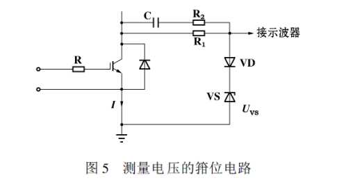
A complete observation of the voltage during IGBT turn-on and turn-off can be done directly using the oscilloscope probe, but for IGBT voltage tailing and on-state saturation voltage drop during turn-on, a clamp circuit is required (see Figure 5). The reason is that the oscilloscope's Y-axis resolution should be set to 0.5/div~10/div, and the input probe's voltage can vary from a few hundred volts. In this case, the oscilloscope usually produces a large amount. Distortion, zero drift, cannot be observed normally. Using the voltage clamp circuit consisting of R1, R2, C, VD and VS in the figure, the part of the Uce that is smaller than UVS can be taken out. Observed with an oscilloscope without distortion and drift. The relationship between UVS and Uce can be expressed as:
When measuring the Uce opening and tailing process, UVS = 50 V should be selected. When measuring the dynamic saturation pressure drop, UVS = 12 V should be selected.
In the figure, R2 and C are used to compensate for the distortion caused by the oscilloscope probe input capacitance and VD and VS junction capacitance. The clamp circuit is calibrated using a known square wave signal prior to use.
Application examples
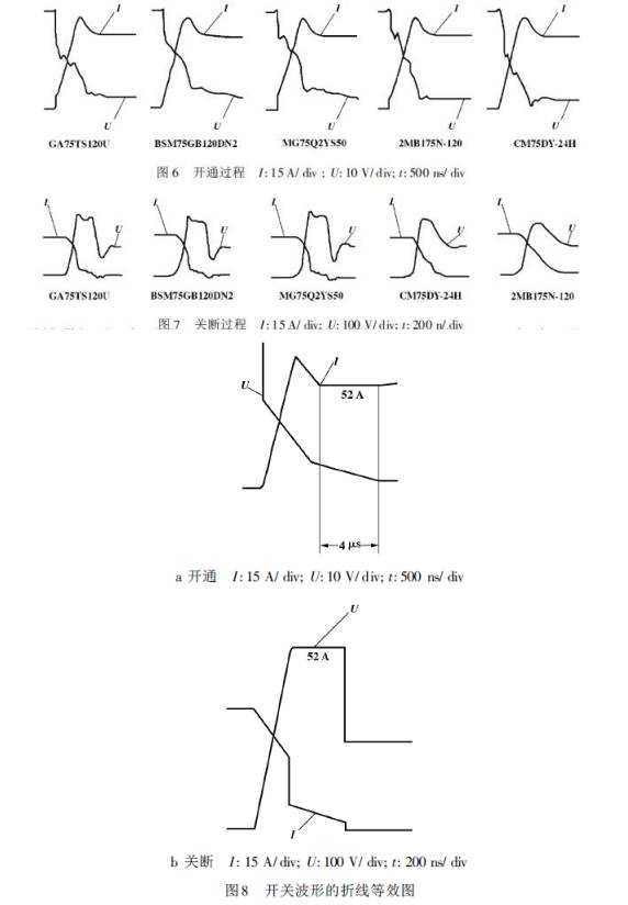
The waveforms in Figures 6 and 7 are measured when different IGBTs are operating in the circuit shown in Figure 1. The measurement conditions are: input voltage Ucc = 520 V, output power Po = 11 kW, primary current I = 52 A, operating frequency f = 20 kHz. The turn-on voltage measurement in Figure 6 uses the clamp circuit in Figure 5, with a clamp voltage value of UVS = 48 V, so the maximum voltage on the waveform does not exceed 48 V.
The measured waveform is line-equivalent, and the integral of the voltage and current is integrated to calculate the total loss of the IGBT. Figure 8 is the equivalent diagram of the GA75TS120U switching process, and thus obtains:
Opening loss: P1 = 12 W
Turn-off loss: P2 = 56.6 W
Transition loss: P3 = 10 W
On-state loss: P4 = 53.8W (saturation pressure drop Usat = 2
Total single tube loss: P c = 132.4 W
The saturation voltage drop Usat, which calculates the on-state loss, is measured using the clamp circuit given in Figure 5, with the clamp voltage UVS = 12 V.
It can be seen from the waveform that the saturation pressure drop has a transition process from turn-on to stability, and the resulting loss P3 cannot be ignored.
The following table shows the results obtained by measuring the IGBTs of several different companies by the above method; the measurement circuit is shown in Figure 1, and the measurement conditions are the same.
Measurement results can be used as a basis for selecting IGBTs and thermal designs. For the selection of IGBTs, switching losses and on-state losses should be considered. When operating at low frequencies, the total loss of IGBTs with low saturation voltage drop is small, while for high frequency operation, IGBTs with fast switching speed should be selected.
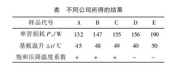
It is worth noting that Sample A (IR Company GA75TS120U) has a lower saturation voltage drop in high speed IGBTs and therefore less total losses. At the same time, it can be seen from the table that the loss of sample D is close to that of B and C, but the substrate temperature is lower; the loss of sample E is larger, but the substrate temperature is not significantly higher than B and C, which indicates the heat of samples D and E. The cycle ability is poor. Although the junction-shell thermal resistance Rth( j- c) indicated in each IGBT data sheet in the sample is basically the same, Ucc= 520 V, Po= 11 kW, I c= 52 A, f = 20 kHz, NPT are usually used. The die (GA75TS120U) manufactured by the (non-punch-through) technology is only one-fourth the thickness of the PT (punch-through) technology die, so the thermal resistance is small and the thermal cycle capability is strong, which can reduce the requirements for the heat sink. The switching speed does not change with the junction temperature. The switching speed of PT type IGBTs decreases with increasing temperature. NPT type IGBTs can be considered for high frequency operation.
to sum up
The loss measurement analysis method described in this paper is simple and effective, which enables designers to make a selection of IGBT selection and thermal design in order to obtain an optimal design. It should be noted that the standards of the measuring tools and auxiliary circuits are very necessary, otherwise it may lead to large errors.
At present, flat Zinc bar is the ideal material for the zinc static and dynamic balance block of vehicle wheel, with good corrosion resistance.
Excellent mechanical properties,elongation is up to 20% or more,the yield of balance pieces stamping is high.
Product specification: Ñ„19mm(width)*2.65mm(thick)
Product packing: 30-150kgs(special packaging specifications can be negotiated)
Flat Zinc Bar,Anode Zinc Bar,Galvanized Zinc Flat Bar,Zinc Coated Steel Flat Bar
Shaoxing Tianlong Tin Materials Co.,Ltd. , https://www.tianlongspray.com