Microelectromechanical systems (MEMS) will soon become an integral part of intelligent system design and construction. These devices shorten the gap between the physical world and the electronic world, and they are used in a wide range of applications, covering a variety of market segments. In many market segments, price reductions, increased accuracy requirements, and rapid market demand will place new constraints on design and manufacturing performance. To succeed, companies must find new ways to meet these challenges.
The increasing complexity of such products requires a design flow that allows engineers to simulate the entire manufacturing process, all environmental and operating conditions of the entire multimode system before constructing the actual silicon wafer. This enables engineers to quickly and aggressively optimize designs to maximize system accuracy and reliability while minimizing output losses due to process variations and other unforeseen interactions.
Accurate statistical converter models for collaborative simulation and their associated signal processing and control security are essential for building robust design flows for intelligent systems. Converter model generation can be a time-intensive task, especially for new structures with unique geometric properties or equations of motion with second-order effects that are difficult to find in analytical equations. Progress in the field of model reduction (MOR) specifically addresses these challenges [1-2].
In the past, the electromechanical behavior of MEMS components has been analyzed using traditional finite element and boundary element methods. Commercial 3D solvers allow very accurate and very detailed simulations of the physical behavior of MEMS converters, so they tend to be the tools of choice for MEMS component designers. However, such simulations are extremely time consuming, and the functions for running coupled field analysis are still limited, and it is not easy to allow co-simulation with interface electronics, so they have little effect in optimizing and characterizing the entire system.
A common approach is to generate a library of MEMS elements that can be assembled to build a schematic of a MEMS device [3]. These subelements may be derived from theory, experimental results, or FEA simulations. This approach is very useful for architectural analysis because it allows designers to quickly discover the effects of changes in the nominal converter design, but it does not always capture the true flexibility of the relevant subject, especially when the child elements are considered rigid. time. This can lead to an overestimation of the stiffness of the structure and the danger of ignoring the critical inherent modes that may actually impede the normal operation of the entire system.
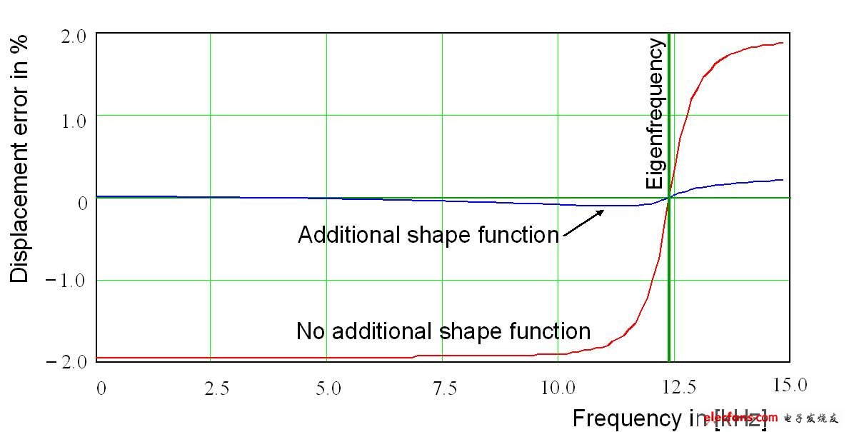
In order to accurately model the inherent flexibility of the microstructure and capture second-order and nonlinear behavior, a more appropriate reduced-order modeling approach is needed. One method is modal superposition, which provides the most efficient representation of the converter. Modal superposition uses the lowest number of state variables to capture the true elasticity of the structure. Speed ​​and accuracy are easily balanced by changing the number of eigenmodes included in the model generation process. An additional shape function (addiTIonal shape funcTIon) can be added to improve the accuracy of the system simulation. Figure 1 shows an example of how to use modal superposition and additional shape functions to achieve the expected accuracy of the package effect on the converter [4]. Extracting models and frequencies from laboratory measurements is easier than determining stiffness, so silicon verification for this model is straightforward. This highly accurate reduced-order modeling approach should be used for low-level testing of components and systems, and must be combined with statistical modeling of manufacturing distributions.

Figure 1: Using modal overlays and additional shape functions to improve the accuracy of reduced-order modeling
Ideally, 'point' or non-extended modeling solutions should be avoided as they limit the designer's ability to explore and optimize the design space at the system level. The model should parameterize the geometry, flow, and environment variables of the size signal behavior.
The converter model is really useful only when the manufacturing distribution of the component is accurately expressed. Process variables, such as changes in film thickness and etch bias, can cause converter behavior changes that must be signaled and adjusted at the system level. Underestimating this change may result in output loss in the final test, while overestimation may result in a conservative design that reduces gross margins.
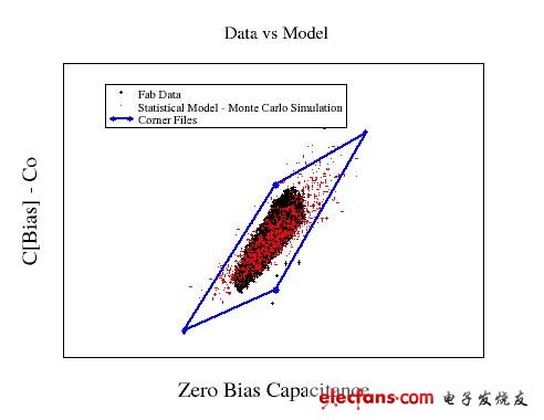
Solid statistical modeling is possible as long as the basic equations of the core modeling accurately capture the effects of physical variables on the behavior of the converter. Statistical distributions are easily obtained from manufacturing targets or by sampling actual manufacturing data using methods such as backward propagation variables (very well known in the IC industry) [5]. The benefit of obtaining statistical data from the metrics actually measured during the casting process is the ability to provide a long-term method of verifying the design environment and manufacturing distribution consistency. Figure 2 shows an example of a comparison of silicon data and statistical modeling for a particular converter test condition. The angular file contains statistical modeling results for specific sigma levels.

figure 2
Regardless of the particular method used to build the converter model, model generation automation is critical to shortening the design cycle to the level required to compete in today's marketplace. To meet current and future product design needs, commercial tools for MEMS system design must provide methods to directly derive results from the converter designer's finite element environment and use the results for generation by system and circuit designers in industry standard analog IC designs. The compact converter model used in the process. This approach will reduce cycle time, reduce errors, and allow for innovation in the design cycle.
MEMS models are used by system and IC designers, so models should be integrated as closely as possible into the user's design flow. For IC designers, this requires the model to support all simulators, with multiple views of various materialization levels in the design flow. Achieving this is not an easy task, and you need to consider best practices for quality assurance, model validation, and lab management. If a special method is used, the use of the model will be impaired. To facilitate greater structuring of the modeling process, companies should adopt design kits. These kits are similar to the standard IC design kits offered in the foundry, performing the best methods mentioned.
Sensor companies should expect to increase any commercial tools available today and for the foreseeable future. The tools and methods used in the MEMS design flow must support automated model generation, variable parameterization relative to system performance, scalable models, and IC design process integration. But the most obvious is the need to invest in building a reliable statistical model that captures the manufacturing distribution and keeps the design environment consistent with the manufacturing site. The MEMS process that captures all of the elements discussed is critical to achieving the best solution for next-generation sensor products.
Directional Antenna WiFi,Directional Antenna TV,Directional Antenna LTE,Directional Antenna Indoor,Directional Antenna Outerdoor
Yetnorson Antenna Co., Ltd. , https://www.yetnorson.com