Boost boost circuit English name is "theboostconverter", or "step-upconverter", is a switching DC boost circuit, which can convert DC into another fixed voltage or adjustable voltage DC, also known as DC - DC converter (DC/DCConverter).
The DC-DC converter intermittently controls the DC voltage to the load through the on-off control of the power electronic device, and changes the average value of the output voltage by changing the duty ratio.
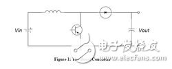
Assuming that the switch (triode or mos tube) has been disconnected for a long time and all components are in an ideal state, the capacitor voltage is equal to the input voltage.
The switching transistor Q is also in the PWM control mode, but the maximum duty ratio Dy must be limited, and Dy=1 is not allowed to operate. The inductor Lf is a boost inductor on the input side.
Boost circuit structureThe Boost circuit of UC3842 is taken as an example to introduce the structure of the Boost circuit.
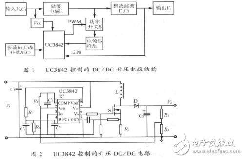
In the figure, the input voltage Vi=16~20V is supplied to the chip and is supplied to the boost converter.
The switch tube is opened and closed at a frequency cycle set by UC3842, so that the inductor L stores energy and releases energy.
When the switch is turned on, the inductor is charged at Vi/L and the energy is stored in L. When the switch is turned off, L generates a reverse induced voltage, and the stored electric energy is discharged to the output capacitor C2 at a speed of (Vo-Vi)/L through the diode D. The output voltage is controlled by how much energy is transferred, and the amount of energy transferred is controlled by the peak value of the inductor current.
The entire regulation process is controlled by two closed loops, namely:
The closed-loop 1 output voltage is sampled and fed back to the error amplifier for comparison with the 2.5V reference voltage inside the amplifier to generate an error voltage. The error amplifier controls the change in output voltage due to load changes.
The closed loop 2Rs is the current detecting resistor between the source and the common terminal of the switching transistor. The voltage generated by the current flowing through the inductor L during the conduction of the switching transistor is sent to the noninverting input terminal of the PwM comparator, and the modulation is controlled after comparison with the error voltage. The pulse width of the pulse maintains a stable output voltage. The error signal actually controls the peak inductor current.
How Boost circuits work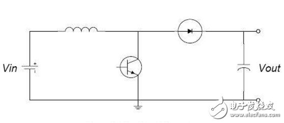
The working principle of the Boost circuit is divided into two parts: charging and discharging.
Charging process
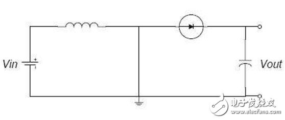
During the charging process, the switch is closed (the transistor is turned on), the equivalent circuit diagram is shown in the figure below, and the switch (triode) is replaced by a wire.
At this time, the input voltage flows through the inductor. The diode prevents the capacitor from discharging to ground.
Since the input is direct current, the current on the inductor increases linearly at a rate that is related to the inductor size.
As the inductor current increases, some energy is stored in the inductor.
Discharge process
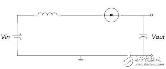
As shown in the figure, this is the equivalent circuit when the switch is turned off (triode cut-off).
When the switch is turned off (triode cut-off), the current flowing through the inductor does not immediately become zero due to the current holding characteristic of the inductor, but slowly becomes zero when the charging is completed.
The original circuit has been disconnected, so the inductor can only be discharged through the new circuit, that is, the inductor starts to charge the capacitor, and the voltage across the capacitor rises. At this time, the voltage is already higher than the input voltage. The boost is complete.
The boosting process is an energy transfer process of an inductor. When charging, the inductor absorbs energy, and the inductor emits energy when discharged.
If the capacitance is large enough, a continuous current can be maintained at the output during the discharge.
If this on-off process is repeated, a voltage higher than the input voltage can be obtained across the capacitor.
We can follow customers' drawings or design to make Customized wire
harness for various industries: game machine, ATM, POS machine, etc.
Customized wire assembly with AVL components from original manufactures. Also harness with local equivalent componets are workable with short L/T and competitive price, also flexible MOQ.
Medical Wire Assemblies,Medical Alligator Clip Cable,Medical Cable Assembly,Medical Wire Harness,Medical Cable
ETOP WIREHARNESS LIMITED , https://www.wireharnessetop.com