In recent years, with the advent of LED luminaires, revolutionary changes have taken place in the field of lighting. In European and American retail stores, ancient incandescent bulbs are hard to trace and even prohibit sales. In the alternative lighting market, low-power compact fluorescent lamps (CFLs) are now facing new competitors. LED technology is constantly improving, and LED luminaires are becoming increasingly powerful in terms of brightness and power. These features, combined with their unique energy efficiency, make LED luminaires ideal for lighting.
Generally, incandescent bulbs produce 10 lumens per watt, while LED manufacturers claim that LED fixtures can reach up to 100 lumens per watt. However, the limitations of form factor and maximum operating temperature make it difficult for LEDs to reach their full potential. The best-performing LED replacement luminaires currently have an efficiency of 50-60 lumens per watt. As a result, LED luminaires are already indistinguishable from CFL luminaires in terms of efficiency standards (Note: CFL lamps have an efficiency range of 60-70 lumens per watt and limited potential for improvement).
Ecological issues are also receiving increasing public attention. As people's awareness of environmental issues such as global warming and climate change continues to increase, the concept of saving resources and energy is becoming the focus of many marketing strategies. The reduction in vehicle fuel consumption and the ban on incandescent lamps over the past 10 years are a good illustration of this trend. Multinational governments around the world have set a timetable for the elimination of incandescent lamps. There are also public policies that provide loose tax support or other financial assistance for energy-efficient “ecological†products.
The inherent advantages of LEDs are in line with the public's eager anticipation for safe, energy efficient and environmentally friendly lighting solutions. LEDs have many other advantages, such as higher dimming capability, longer life and smaller form factor, opening the door to shape, color, longevity and cost.
Replacing traditional lighting sources (fluorescent, CFL, halogen or other incandescent) with LED lighting solutions that are compatible in mechanical, optical, electrical and thermal aspects is an ongoing industrial revolution. The business, office and residential lighting markets call for high quality LED retrofit lamps. Although cost issues remain a major obstacle to these solutions, there are also technical issues to be aware of:
[1]. Electrical compatibility with existing infrastructure, especially when using standard in-wall outlet dimmers.
[2]. The shape must be screw type
[3]. Must solve the heat dissipation problem of LED
1.1 Dimmer compatibility
Currently, control devices for lighting fixtures in homes, hotels, and offices are designed for incandescent lighting. The best way to provide dimming is to use a "mains phase cut" dimmer. This dimmer was developed in principle for powering incandescent lamps. From an electrical point of view, an incandescent lamp can be considered as a resistive load.
The electrical equivalent load of an electronic lighting source (such as a CFL energy saving lamp or an LED lamp) is no longer a purely resistive load. This makes a big difference in how the dimmer works. Improper use of the load can cause the system to malfunction, and can cause very uncomfortable flicker or even damage to the fixture or dimmer. This may cause user dissatisfaction and delay the adoption of LED solutions. Currently, dimmers are still expensive and difficult to install. Therefore, the introduction of quality solutions compatible with existing dimmers has become a necessity to realize the promise of LED lighting promotion.
Although the phase-cut dimmers are of different types, the working principle is basically the same (that is, some power supply sine waves are cut off in each cycle). This can be done with a switch. When the switch is turned on, the power is delivered to the load (bulb). When the switch is turned off, no power is supplied. By adjusting the switch on time, the total energy supplied to the load can be adjusted.
What Does PCB Assembly Mean?
PCB Assembly Service in China
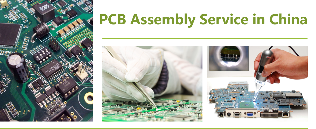
Although there are many companies in the United States, Britain, India, Australia, Canada, Mexico, Taiwan, Malaysia, Thailand, Germany, Romania and other local selection of PCB assembly manufacturers, but they are not cheaper than assemble in China, because China's PCB assembly cost is lower, better quality.
Why Choose US for PCB Assembly Services - Turnkey, Quickturn PCB Assembly Service
|
Turnkey Services |
Instant Online Quote |
Affordable Pricing |
|
Contact our online customer service or send us an email.
We offer 7*24 hours of online real-time quotation and online customer support. |
We have many years and rich experience in PCB production and assembly. There are very professional technicians and operators, with very advanced PCB assembly process, they are the guarantee of product quality. On this basis, we can also provide you with cheaper, better quality products. |
|
Quick-Turn assembly |
100% Quality Guarantee |
Mature Capabilities |
|
Get the entire PCBA produced in 20 working days from order confirmation to dispatch, including sourcing of parts. However, if you need faster delivery time, we can do it, but you may need to pay an additional premium. |
100% quality guaranteed - free re-work if needed. All parts are sourced from reliable suppliers, and each board undergoes free visual inspection. X-ray inspection, AOI testing, In-Circuit Testing (ICT), and functional testing are also available. |
JHYPCB's assembly lines are fully compliant with IPC-A-610F, are capable of SMT, through-hole and mixed assembly, and can solder BGA and fine-pitch components from 0.38mm pitch. PCB types include rigid, flexible, rigid-flex and aluminum boards. |
|
Prototype, Small or Large Batch |
Sourcing Options |
Considerate Customer Service |
|
Whether you need prototype PCB assembly or bulk assembly, JHYPCB can cater for as little as a single piece 1 to 10000 pieces and has dedicated assembly lines for both low and high volume needs. |
We can source components from reputable distributors, or you can choose from us. These parts are cheaper and can reduce the entire PCBA production time to 7 working days. |
Every PCBA order is assigned a project manager to assist you with the order process. The engineering and assembly teams will also communicate any issues with you to ensure your order proceeds as planned. |
PCB Assembly Capabilities
- Prototype PCB Assembly as Quick as 1 Day
Our printed circuit board assembly service is North America's leading one-stop solution for PCB and assembly under one roof; specializing in small and medium runs with fast lead-times and no minimum quantity requirements.
- A Seamless Process from PCB fabrication to PCB Assembly
All printed circuit boards assembled by Advanced Circuits are made by Advanced Circuits and we maintain full control of the entire process so you don't have to manage multiple vendors. When you choose Advanced Circuits, you can be sure that your PCBs flow directly into our in-house Assembly Department to begin assembly without delay.
- Assembly Types
- Surface Mount (SMT) Assembly
We are capable of small volume SMT prototyping PCBs with both automated and manual assembly.
- Ball-Grid-Array (BGA) Assembly
We are equipped with advanced automated BGA placement equipments as well as X-ray inspection equipments to guarantee the quality of BGA assembly.
- Through-Hole Assembly
Components are placed by inserting leads into holes that covered with solder.Both automated and manual through-hole assembly are available.
- Mixed Assembly
Both SMT and Through-Hole components will be placed on the PCBs.Single or double side mixed assembly is available.
- Kit Assembly
PCB Types for Assembly
- Prototype PCB Board
- FR4/ Rigid PCB Board
- Aluminum PCB Board
- LED PCB Board
- Flexible PCB Board
- Rigid Flex PCB Board
- Solder Types
Lead-Free (RoHS compliant)
- Assembly Time
From 8 hours to 72 hours once all parts are ready
- Component Types
- Ball-Grid-Arrays (BGA) of 0.25mm pitch with x-ray testing
- Passive components as small as 01005 (0402) package
- Fine-pitch components as small as 0.38mm pitch
- Test Types
- Visual Inspection
- X-Ray Inspection
- AOI Testing
- In-Circuit Test
- Functional test
- Component Suppliers
- More than 10,000 in-stock components (OPL)
- Digikey, Mouser, TME, Element 14 and more-
- PCB Assembly Testing Capabilities Learn More
| Category | Product Function | Test Type | Test Location |
|---|---|---|---|
| MCU |
51 serial MCU AVR serial MCU ARM Cortex M0, M0+, M3 and M4 serial |
IC Programming | Seeed's Fab |
| General |
GPIO Functional Testing Voltage, Electricity Current, Resistance Test, etc. I2C/Uart/SPI/CAN/One Wire/SWD Temperature, Humidity, Atmospheric Pressure etc. ... |
Functional Test | Seeed's Fab |
| Communication |
GSM/WCDMA/LTE GNSS Bluetooth/LE Ethernet NFC 802.11/b/g/n/a/ac ZigBee Sub-1 GHz 315/433/868/915 |
Functional Test | Seeed's Fab |
| Monoboard Computer | BeagleBone, Raspberry Pi, etc. | Functional Test | Seeed's Fab |
| Certification | FCC, CE, GS, TELEC etc. | Regulatory | Accredited Third-Party Lab |
PCB Assembly Applications
 |
 |
 |
 |
|
Aerospace |
Automotive |
Biomedical |
Consumer-electronics |
 |
 |
 |
 |
|
Energy |
Industrial |
Network-computer |
Telecommunications |
PCB Assembly Manufacturing Design Tips

- Choosing between ROHS (LEAD-FREE) or standard (LEADED) solder
RoHS is used most frequently when shipping to Europe. As RoHS and Leaded solder temperatures are different, boards must either be completely soldered with RoHS or Lead. This includes BGAs. Non-RoHS components can withstand RoHS process. Avoid mixed process; that is, mixed solder. For example, a standard HASL bare board should not use a RoHS assembly process.
- Water Clean
Use No Clean Flux only if your PCBA has some parts (batteries, microphones, speakers, relays, etc...) that can be damaged if submerged in a water wash. No Clean Flux leaves flux residue on the finished PCBA; however, flux is non-corrosive and non-conductive.
If a few components are water sensitive, you may choose to have the PCBAs processed with water soluble flux without initially soldering the water sensitive components. Make sure include specific instructions to hand solder these few components after cleaning with No Clean Flux.
- Silkscreen
- Placement (X-Y) Centroid Files
- Shortages
- Fiducial
- Moisture Procedure
- Paste Layers
- Multi-part Assembly orders
- Substitutions
PCB Assembly Cost
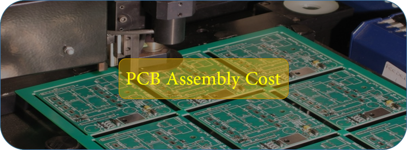
PCB Assembly Cost = PCB manufacturing cost + PCB frame test or flying probe test fees + PCB engineering cost (only for small prototype order) + Component cost (additional 5%) + SMT assembly charges + PCB assembly test cost + Box building charges + Package cost (for special application) + Logistics cost (requested)
PCB Assembly Process
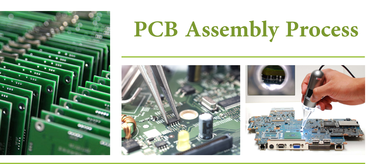
PCB Assembly Process
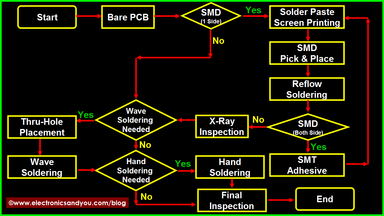
PCB Assembly Process Flow Chart
Things Needed for Printed Circuit Board Assembly
Following electronics parts and consumables are needed for PCB assembly
- Printed Circuit Board
- Electronic components
- Soldering materials including solder wire, solder paste, solder bar, solder preforms (depending on the type of soldering to be done)
- Soldering flux
- Soldering equipment including soldering station, wave soldering machine, SMT equipment, inspection and testing equipment etc.
Once all of the above equipment, electronic parts and all raw materials are arranged, it is time to start the printed circuit board assembly process.
1. PCB Manufacturing
PCB design & fabrication helps you with experienced PCB design and fabrication, high accuracy, quality control. In general, your PCB Prototype can be well served by us. PCB Assembly includes layout, fabrication and assembly. We also have monthly abilities of offering 35,000 square meters PCB, 80 million point SMT and introduce ICT, flying probe, AOI, X-ray, function test, burn-in test into inspection phase. We can help you with a system of transforming natural resources, raw materials and components into a finished product that is delivered to the end customer and strive to have the most optimized supply chain to make efficient and costs lower.
2. Screen Printing of Solder Paste onto PCB Board
loctite solder pastePhysicochemical and process property of solder paste directly impact SMT soldering quality. Solder paste printing is applicable for placing appropriate amount solder paste onto PCB pads, in order to ensure good circuit connection between SMT components and PCB pads and their mechanical strength. Solder paste printing is the critical process of SMT. Metal template printing is conventionally applied so far. According to related statistics, 60%~70% quality problems are caused by solder paste printing in premise of quality guarantee of components and printed circuit board. Requirements of solder paste printing:
a. Place solder paste appropriately, evenly and uniformly. Solder paste shape is clear and neighbor shapes do not connect. Solder paste shape is in compliance with that of pad, without any dislocation.
b. In general, the unit area solder paste amount should be 0.8mg/mm2, particularly 0.5mg/mm2 for narrow-pitch components.
c. After solder paste printing, the shape has no heavy collapse and edges are trim. Plate surface is not allowed to be contaminated by solder paste.
There are a large variety of solder paste with different alloy compositions, granularity and viscosity even for all from one manufacturer. How to choose appropriate solder paste highly impacts the product quality and cost. Now NOD Electronics is using Loctite lead free solder paste. We have figured out Loctite solder paste is reliable to ensure good product quality after process engineering test of its printability, demoulding, thixotropy, cohesiveness, wettability, welding spot defect and residue.
3. Lead-free PCB Assembly
In light of environmental concerns and customer request, we can offer lead-free PCB board assembly which complies with RoHS standards. At upstream, we choose PCB laminates in compliance with RoHS standards for PCB manufacturing. Also we use lead free solder paste and related reflow/wave ovens. We strictly fulfill RoHS requirements in light of your local regulations and don`t want to make you into any trouble on this basis.
4. Burning Program and In-Circuit Test (ICT)
Our test engineers will check short circuit, voltage, current, signal transmission of PCB assembly boards according to your ICT test plan. A professional report will be handed up to you if for any detected problems. For batch order, we design exclusive test frames to fast the ICT test process. We are also well sophisticated with decoding and burning program for you. Related test frame will be built to ensure products work effectively according to your requirements.
PCB Assembly Requirement List
| No. | Types Of Assembly | File Format | Component Footprinr | Component Package | Testing Produres | Produres | Others |
| 1 | SMT ASSEMBLY | Gerber RS-274X | 0201,0402,0603- | Reels Package | Visual Inspection | Lead-Free(Rohs) | Custom Reflow Profile |
| 2 | SMT & THT Assembly | BOM(.xls,.csv,.xlsx) | BGA,QFN,QFP,PLCC | Cut Tape Package | X-Ray Inspection | Leaded Solder | Standard Reflow Profile |
| 3 | 2 sided STM,THT Assembly | Pick-N-Place/XY file | SOIC,POP...Connectors | Tube and Tray | AOI,ICT(In-Circuit Test) | Reflow Soldering | Smallest Size:0.2"x0.2" |
| 4 | Mixed Assembly | - - | Small Pitch of 8 Mils | Loose parts and bulk | Functional Testing | Wave Soldering | Largest Size:15"x"20 |
Find Out More
Flexible PCB Circuit Board Assembly
Through Hole Technology Assembly
Mixed Technology PCB Assembly
Double Sided PCB Assembly
Learn More Information
How to Mixed Technology PCB Assembly
Comparison between THT Assembly and SMT Assembly
How to start to Prototype PCB Assembly
Introduction About Single-sided and Double-sided SMT Assembly
How to ensure a smooth PCB assembly
How to Reduce PCB Assembly Cost
PCB Assembly Service
Printed Circuit Board Assembly, PCB Assembly Service, PCB Assembly
JingHongYi PCB (HK) Co., Limited , http://www.pcbjhy.com