Despite the emergence of power semiconductor components such as power field effect VDMOS and insulated gate bipolar transistor IGBTs, and occupying an important position in the field of power electronics technology, thyristors (thyristors) are still stable due to their high voltage and high current resistance. The position is favored by users. In the case of abandoning the current sampling, amplification and execution, the transistor error amplifier in the single-junction phase-shifting flip-flop is changed to an integrated operational amplifier, and the over-current and short-circuit protection of the thyristor DC voltage regulator can be realized. The circuit structure is simplified, and the stability reliability and AC-DC conversion efficiency of the whole machine are improved.
working principleThe control circuit of the error amplifier using the thyristor DC regulator of the integrated op amp is shown in Figure 1. The controlled main circuit (not shown) is a three-phase half-controlled rectifier bridge, and then an LC smoothing filter, output + 12. 8 V smooth DC voltage. The three thyristors in the three-phase half-controlled rectifier bridge are respectively triggered by the pulse transformers T2a, T2b and T2c in the illustrated control circuit. The three phase-shifting trigger circuits that drive the three pulse transformers are identical and share an error amplifier and its voltage sampling circuit. To avoid repetition and cumbersomeness, only the phase-shifted flip-flop circuit of phase B is shown in the figure, and the phase A and phase C circuits are summarized by dashed lines.

The phase shifting flip-flop circuit still uses the conventional single-junction transistor phase shifting flip-flop. That is, when the cathode voltage of the diode VD3 rises, the current flowing through the transistor VT2 (i.e., the charging current of the capacitor C1) decreases, the pulse voltage output from the single junction transistor VT1 shifts back, the conduction angle of the thyristor decreases, and the output voltage decreases. When the cathode voltage of the VD3 tube drops, the current in the VT2 tube increases, the charging speed of C1 increases, the pulse voltage of the VT1 tube advances, the conduction angle of the thyristor increases, and the output voltage also increases. However, the maximum current in the VT2 tube is limited by the resistance of resistor R3, and it is impossible to increase without limit, that is, the maximum conduction angle of the thyristor will be locked by R3 to a value less than 180° greater than 0°.
By replacing the transistor error amplifier with an operational amplifier-type error amplifier, the circuit structure will be simplified, and the magnification can be easily adjusted. It is easy to make a proportional integral derivative adjuster (PID), which makes the dynamic characteristics of the voltage regulation system more perfect and reasonable. The VD2 tube isolates the smooth DC voltage of C2 from the synchronous trapezoidal voltage on the phase shifting trigger. When the output voltage of the + 12. 8V from the main circuit changes, the voltage on the sampling potentiometer RP also changes proportionally, so that the voltage of the pin 3 of the non-inverting input of the op amp N changes accordingly, and the voltage of the pin 6 of the output terminal is amplified according to the amplification factor. The change eventually causes the thyristor output voltage to change in the opposite direction, balancing the changes at the output of the main circuit and maintaining the output voltage stable.
When an overcurrent or short circuit occurs at the output of the main circuit, the output voltage will at least have a large drop. The resistance of R3 limits the maximum conduction angle of the thyristor. Even if the thyristor has reached this maximum conduction angle, it cannot compensate the voltage drop generated by the overcurrent on the main circuit, so that the output of the main circuit + 12. 8 V Severe drop (voltage is 0V when short circuited). In this way, the voltage of the 3-pin input terminal of the op amp N is lower than the inverting input terminal 2, so the output terminal 6 outputs an ultra-low voltage, a large current flows through R3, and the collector voltage of the VT2 tube is lower than the single-junction transistor VT1. The peak voltage, the VT1 tube can not generate oscillation pulses, the three thyristors in the main circuit can not be turned on, achieving overcurrent (short circuit) protection. At the same time, the buzzer HA sounds and the LED VL lights up, informing the operator in the form of sound and light that it is in an overcurrent (short circuit) protection state.
After the load is faulty, press the recovery button SA, the DC voltage on C2 is re-energized through resistor R7 to make the voltage of pin 3 of the op amp N higher than 2 pin, 6 pin output higher voltage again, the thyristor returns to conduction, + 12. 8V The output voltage returns to normal. Capacitor C3 is the starting capacitor. If there is no C3 at the instant of power-on, there is no DC voltage output in the main circuit. The voltage of pin 3 of the op amp N is zero, and the voltage of pin 2 is higher than 7 V, so the voltage of pin 6 of the output terminal is very low. 2V), the voltage on the capacitor C1 does not reach the peak voltage of the VT1 single junction transistor, the VT1 tube has no pulse voltage output, the thyristor cannot be turned on, and the output of the main circuit will be in the zero voltage state. After setting C3, the synchronous voltage at the startup is charged to C3 through the VD2 tube, and the voltage at pin 2 is higher than that of the op amp N in RP and R11, and the higher voltage is output at the 6th pin, so that the output of the main circuit outputs +12. 8 V. DC voltage.
It is not difficult to see that this circuit is similar to the collector output transistor DC regulator, but the circuit is superior - it can be started by only one capacitor, and does not affect the regulation performance.
Circuit debuggingWhen the circuit is connected to the main circuit for debugging, it is possible to change the resistance of the resistor R3 to a larger value, and then gradually increase the load at the output of the main circuit. If the output voltage suddenly drops to zero when applied to a current below the set protection current value, this indicates that the overcurrent protection function has been implemented, but it has been implemented too early. At this time, the resistance of R3 can be reduced. Continue the loading experiment as before. The protection current action value should be larger than the last time. Continue to reduce the R3 resistance until protection is achieved when the set protection current is reached. After the R3 resistance is confirmed, when the fixed resistor with the same resistance is used, the potentiometer should be used as much as possible to avoid the loss of the resistance value or the overcurrent (short circuit) protection function, which hinders the normal application of the regulator.
As we all know, the trigger power of a single-junction transistor type flip-flop is not very large. The application circuit described in this paper is used to trigger a three-phase half-controlled thyristor bridge rectifier. The thyristor specification is 100A, so that the output current of the +12.10V regulator can be Up to 180A, when over 180A, the hidden overcurrent (short circuit) protection function appears—the single-junction transistor VT1 loses the oscillation pulse and the three thyristors are turned off. The capacity and rated voltage of the three-phase power transformer (not shown) in the main circuit determine the upper limit of the current action value to be protected. As for the value below the upper limit, it is determined by the resistance of the resistor R3. Decide. In fact, the parameters of the single-junction transistor VT1 and the triode VT2—such as the voltage divider ratio, peak voltage, valley voltage, current amplification factor, etc., together with the R3 resistance value, determine the protection current action value, but VT1 The VT2 tube parameters are highly discrete. Generally, only the method of adjusting the resistance value of R3 is used to determine the action value of the protection current, which is more convenient and economical. This is not difficult to understand: why the same type of regulator of the same model will have different R3 resistance. For the same regulator, the parameters of the single junction VT1, transistor VT2 and resistor R3 of the three flip-flops should be consistent to ensure uniform (symmetric) and optimal conduction angles of the three thyristors. Ripple factor.
Considering that the voltage regulator has a certain requirement on the ripple coefficient of the output voltage, and the filter inductor cannot be set too large, the controllable range of the output DC voltage should not be too wide, at the lower limit of the supply voltage and the output rated current. When the output rated voltage (such as + 12. 8 V), there is a little adjustment margin above and below, which requires the manufacturer to design the secondary winding of the three-phase power transformer. Then, adjust the resistance of resistor R3 and potentiometer RP during debugging to finally meet the expected output characteristics. Although only a specific practical circuit is drawn in this paper, the circuit form and its working principle are applicable to all phase-shifting thyristor DC voltage regulators. It is not necessary to stick to this "practical circuit" when using it. The idea, with this question, give full play to the results of the design.
ConclusionIn summary, it is not difficult to find that in the control circuit and the main circuit not shown, there is no overcurrent and short circuit protection circuit, and there is no special component with overcurrent protection function, but the overcurrent can be realized. And the reliable protection of the short circuit, and the action value of the protection current can be adjusted in a wide range. This is a thyristor DC regulator with no overcurrent protection but overcurrent protection. It is the result of a reasonable combination of single junction transistor phase shifting flip-flops and integrated operational amplifiers. Through this example, some inspiration can be obtained: the reasonable combination of some components can produce unexpected effects - all kinds of components have more or less hidden functions like this. In a sense, the significance of actively developing the latent functions of components will even exceed the development of new components. It's like making a new combination of the same text and writing another article with a deep and interesting mood. I hope this article can play a role in the more new applications of traditional components.
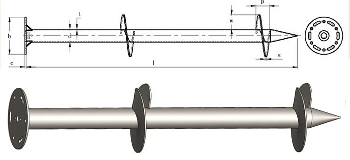
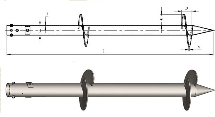
Hot dip galvanized Ground Screw Pile ,Screw Pile ,Helical Screw Pile foundation materials are carbon steel Q235 (S 235 ) or Q355 ( S350) ,with hot dip galvanized finish treatment .
Helical Screw Pile ,Screw Pile ,Helix Screw Pile with one ,two three or four pieces big blade .blade diameter can be 300mm,350mm,360mm 450mm or any size as customers' design.
Screw pile foundation ,ground pile suitable for soft soil condition .
Screw Pile tube diameter : 76m,89mm,102mm,114mm,219mm.
Helical Screw Pile including Flange ground screw pile ,Flat nut ground screw pile .
Usuage : Screw Pile used in many fields ,such as Solar mounting system ,PV mounting ,fence ,housing construction ,road signs ,highway guardrail ,flagpole & .


Screw Piles ,Helical Screw Pile ,Screw Pile Foundation,Screw Pile Cost
BAODING JIMAOTONG IMPORT AND EXPORT CO., LTD , https://www.chinagroundscrew.com