 Signal integrity refers to the quality of the signal in the circuit system. If the signal can be transmitted from the source to the receiver without distortion in the required time, the signal is said to be complete. With the rapid development of semiconductor technology and the increase in output speed of IC switches, signal integrity issues (including signal overshoot and undershoot, ringing, reflection, crosstalk, and ground bounce) have become one of the issues that must be addressed in high-speed PCB design. . Usually, the frequency of the digital logic circuit reaches or exceeds 50 MHz, and the circuit that works on this frequency accounts for more than 1/3 of the whole system, can call it high-speed circuit. In fact, the harmonic frequency of the signal edge is higher than the frequency of the signal itself, and the fast-changing transitions (rising and falling edges) of the signal cause unintended effects of signal transmission. This is also the root cause of signal integrity problems. Therefore, how to fully consider the signal integrity factors in the high-speed PCB design process, and take effective control measures to improve the quality of the circuit design, must be considered.
 Using the powerful Cadence SPEEC TRAQuest simulation software, using the IBIS model, the signal integrity analysis of high-speed signals is an efficient and feasible analysis method. It can find the signal integrity problem, and do the signal integrity related issues according to the simulation results. Optimize the design, so as to improve the design quality and shorten the design cycle.
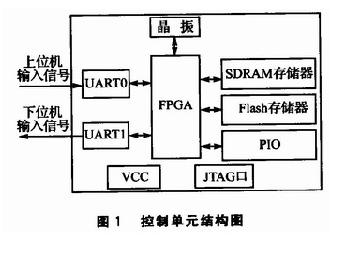
1 Application Design Example The function of the control unit designed in this paper is to transmit the encoded signal received by the ground receiving device back to the master station data processing center. The specific working process is to first store the data of the upper computer, and then through the bit error rate test and calculation, select a path with the lowest bit error rate as the data transmission path, and finally transmit the stored upper computer data to the data processing center of the main station through the path. Processing. After comprehensive considerations, Altera's Cyclone II-2C8 was selected as the core chip, as well as externally extended SDRAM, Flash, various input/output circuits, and MAX232 interface chips, which were combined with the Nios II soft-core processor development kit. The control unit structure is shown in Figure 1.
The clock frequency of CycloneII-2C8 is up to 150 MHz. Since the internal data storage area of ​​the FPGA is relatively small, SDRAM is used to expand the external data storage space. SDRAM uses Hy-nix's HY57V651610/SO with a clock frequency of 75 MHz or more. Therefore, the problem of signal integrity due to high signal frequencies must be considered. The powerful Cadence design software was chosen. It integrates schematic design, PCB layout, and high-speed simulation analysis. It can solve the problems related to electrical performance in all aspects of the design, greatly improving the design. Success rate.
2 key signal topological structure and simulation The higher frequency part in this system is FPGA and SDRAM, FPGA clock frequency can reach above 150 MHz, SDRAM can reach above 75MHz. Because the internal high frequency of the FPGA has no effect on other devices, and the connection between the FPGA and the SDRAM is a seamless connection, the integrity of the signal directly affects whether the FPGA can correctly read and write the SDRAM. In the PCB design, the high-speed simulation tool SPECCTRAQuest of Caden-ce software is used, and the IBIS model of the device is used to analyze the signal integrity and optimize the impedance matching and topology structure to ensure the normal operation of the system. This article only explains the signal reflection and crosstalk in detail. Other simulations are similar to this.
Cutout Fuse Co., Ltd. , http://www.nsindoorfuse.com