In traditional large-scale ASIC and SoC designs, the physical space of the chip can be roughly divided into three parts for new custom logic, for reusable logic (third-party IP or traditional internal IP), and for embedded storage. .
As vendors continue to develop their own custom modules for third-party IP (USB cores, Ethernet cores, etc.) for market differentiation of chip products (for wireless DSP+RF, Bluetooth and other emerging wireless standards for 802.11n) When the CPU space occupied by the CPU/microcontroller core is almost unchanged, the proportion of embedded memory is significantly increased (see Figure 1).
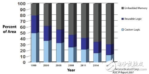
Figure 1: In current ASIC and SoC designs, the proportion of embedded memory in the total available chip space is increasing.
According to data released by Semico Research in 2013, in most SoC and ASIC designs, various embedded memories occupy more than 50% of the chip space. In addition, many large-scale SoC embedded memories have different purposes and main performances. ,as shown in picture 2.
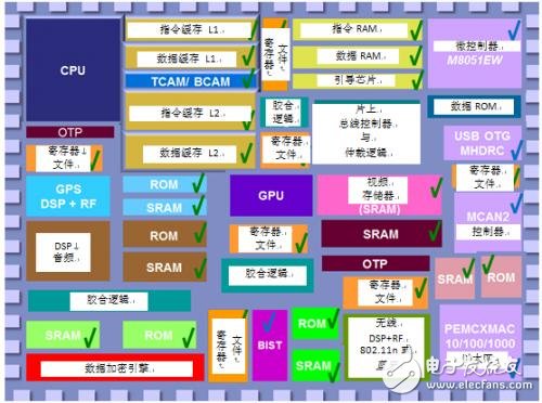
Figure 2: Various embedded memory IPs for multicore SoCs.
Since the design can be optimized by using the correct SoC memory type, it is very important for the designer to utilize various memory IPs. Designers can optimize the performance of various performance parameters such as speed, power consumption, space (density), and non-volatility by properly allocating the proportion of various memory IPs.
Main design criteria for embedded memory
In various application designs, the determination of the optimal memory IP is based on the following five drivers, as shown in Figure 3:
1 power
2 speed
3 reliability / yield
4 density
5 cost
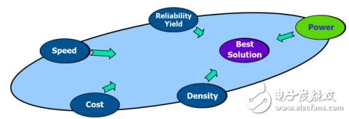
Figure 3: Main factors determining the memory IP.
By balancing the above various performance decision factors, an optimal solution can be obtained. In many cases, the memory compiler automatically generates a specific memory IP that is optimized for performance based on various drivers in the input memory design generation flow. Equally important, the supporting structure of the memory IP should be applied to reliable verification methods, and The generated IP yield is the highest. Finally, to optimize production and quality, the memory compiler should also generate GDSII directly without manual intervention or adjustment. Other elements include good design margin control, support for automatic test pattern vector generation, and built-in self-test (BIST). In addition, it is best to have the ability to debug the silicon through a single step of BIST.
power
Powerful compilers combined with advanced circuit design dramatically reduce dynamic power (CV2f) and can be optimized with multi-chipsets, advanced timing methods, biasing methods, transistor Leff feature control, and multiple supply voltage (VT) Other technologies minimize leakage power. Designers can use these memory technologies in combination to achieve optimal results through voltage and frequency adjustments and the use of multiple power domains.
speed
To achieve first-class memory performance, the full use of advanced design techniques is critical. Designers can use memory compilers to trade off speed (such as access time or cycle time), space, dynamic power, and static power (leakage power) to get the optimal combination. Through the comprehensive selection of various VT technologies, multi-chipsets and various storage units, the memory block can be improved, and the energy-saving design technology can be used to obtain higher speed.
Reliability and yield
The large drop in transistor size and power consumption, while significantly reducing the noise margin, also has an impact on the reliability of very deep sub-micron chips. Therefore, in order to improve the yield and improve the reliability of operation, ECC and redundancy technology are required.
Since the number of bits in SoC is now very large, embedded memory is the most important factor in determining SoC yield. In terms of improving memory yield, proprietary test and repair resources play an important role by reducing batch production time and controlling test and repair costs. The memory IP manufactured by the one-time programmable memory technology can repair the memory array when the storage information fails after the chip is manufactured. Ideally, to quickly fix the program during the production test, the memory compiler's repair function needs to be tightly integrated with the silicon test tool.
It is extremely important for designers to choose to manufacture a unit from a foundry or to design it yourself. Collaborative memory vendors who understand custom designs and provide silicon data for each process node can be a great help when custom design is required. Advanced design techniques maximize yield and reliability even without the need for additional masking and process correction.
density
An important consideration in the choice of memory IP is the ability to select different memory densities for each process node. Advanced memory compilers allow designers to trade off between density and speed, such as whether to select high-density (HD) bit cells or high-current bit cells.
Designers can also optimize SoC layout by controlling memory footprints (variable width, variable height, or square) with features such as flexible column multiplexing to minimize memory-to-chip size. influences. Some memory compilers also support sub-words (bit and byte writable), power grid generation, etc. to maximize power output. In addition, flexible port assignment (one port for read or write and the second port for read and write) also saves space on SRAM, CAM, and register files.
The density relationship between the two embedded memory IP architectures is shown in Figure 4. Compared to a 6-transistor (6T) bit cell, a single-transistor (1T) bit cell can reduce chip space by up to 50% when the bit capacity is constant. In the design, the 1T architecture is an ideal choice when the speed requirements are low and the density requirements are high. The use of a batch CMOS process eliminates the need for additional masking and is therefore beneficial for cost compression. In high-speed applications, designers can use 6T or even 8T-bit units to meet their speed requirements.

Figure 4: The proportional relationship between memory density and different embedded memory IP architectures.
cost
For SoC/ASIC, designers are more willing to choose “space-saving†IP parameters than sub-optimal IP (often referred to as “free IPâ€) to maximize compression costs. Although there are many memory IP parameters that designers can choose for free, there is not always a cost-effective solution for the overall profitability of the product. In many cases, the manufacturing cost is reduced by improving the density and performance of the approved embedded memory IP compared to the "free" memory IP.
The effect of memory volume optimization on mass production costs over the life of the product is shown in Table 1. In this table, the chip space occupied by the memory IP is expressed as a percentage. The cost compression effect of high-density memory can be calculated by chip cost, mass production efficiency, and product life. The saved IP space is derived from Figure 4. As can be seen from the figure, the density increment ratio of 1T and 6T memories is about 2:1.
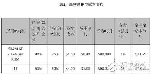
Table 1: High density IP and cost savings.
Embedded Memory IP Selection Guide
To give you an idea of ​​the optional elements in memory design, the types of paid embedded memory with some of the most advanced features are summarized below.
Single port (6T) and dual port (8T) SRAM IP:
Since most of these memory architectures are suitable for mainstream CMOS manufacturing processes, no additional process steps are required, so static RAM memory blocks based on traditional 6T memory cells have become mainstream in ASIC/SoC manufacturing. The 6T memory cell is a proven device for large-scale program or data memory blocks using a proven 6T/8T bit cell from a foundry that can be used in high-speed, low-power designs. The 6T memory cell can be used for storage arrays with storage capabilities ranging from a few bits to a few megabits.
Depending on whether the designer is using a CMOS process optimized for high performance or low power, the memory array with this structure is designed to meet a variety of performance needs. SRAM blocks fabricated in high-performance CMOS processes reduce the access time of advanced process nodes such as 40nm and 28nm to less than 1ns while reducing power consumption. As the process node advances and the form factor shrinks, the static RAM built with the traditional 6T memory cell will have a smaller cell size and shorter access time.
The static nature of the SRAM memory cell allows it to retain a minimum number of support circuits, requiring only the address to be decoded and signaled to the design of the decoder, sensing and timing circuitry.
Single Port (6T) and Dual Port (8T) Register File IP:
This type of register file memory IP is a good choice for fast processor buffers and small memory buffers (up to about 72Kbit per macroblock). The register also has the smallest footprint and the fastest performance.
Single layer programmable ROM IP:
This structure has relatively low power consumption and speed, and is especially suitable for storage of space-limited microcode, storage of fixed data, or storage of applications with steadily increasing volumes. This type of IP supports multiple chipsets and different aspect ratios, reducing both the size of the chip and the optimum speed. To speed up the design cycle, some IPs also provide a programming scripting language to drive the memory compiler.
Content Addressing Memory IP:
This type of IP is mostly used as TCAM (ternary) or BCAM (binary) because it is faster, consumes less power, and takes up less chip space than the algorithmic approach of applications that perform a large number of search tasks. IP for search engine applications. Typically, the search can be done in a single clock cycle. TCAM and BCAM are commonly used for packet forwarding, Ethernet address filtering, routing queries, firmware search, host ID search, memory decoupling, directory compression, packet classification, and multi-way cache controllers.
Single transistor SRAM:
This structure, although slower in speed, is extremely dense and can be used in 180 nm, 160 nm, 152 nm, 130 nm, 110 nm, 90 nm, and 65 nm processes. Especially suitable for ASIC/SoC programs that require a large amount of on-chip memory space - mostly larger than 256Kbit, but do not require extremely high access speeds, and designs with limited space and leakage current in memory blocks. This structure generates a memory array similar to the SRAM operating principle, but is based on a single-transistor/single-capacitor (1T) memory cell (such as used in dynamic RAM).
Due to the 6T memory array, the single-transistor SRAM array has more storage capacity in the same chip space, but it needs to understand the dynamic characteristics of the memory at the system controller and logic level, and play an active role in the refresh control. effect. In some cases, DRAM and its own controllers may be integrated to make it look like an easy-to-use SRAM array. The integration of high-density 1T macroblocks with some of the supporting logic that provides refresh signals allows the dynamics of memory cells to be transparent, allowing designers to treat memory blocks as static RAM when implementing ASIC and SoC solutions.
As a license-available IP, 1T SRAM is available from foundries. However, because some of these IPs require additional mask layers (in addition to the standard CMOS layer), wafer costs are increased, thus limiting the alternative manufacturing space for foundries. In order to make additional wafer processing cost-for-money, the total DRAM array size used on the chip must typically be greater than 50% of the chip space. Most of the available DRAM macros are hard macro cells with limited size, aspect ratio, and optional space for the interface.
There is a special variant of a single-transistor SRAM that uses an architecture that can be fabricated in a standard batch CMOS process, so there is no need to modify the mask or additional process steps. Such IP macroblocks are more cost effective (saving process costs by 15-20%) and can be processed at any factory or changed to a processing plant for cost or production reasons. This solution offers a variety of sizes, aspect ratios, and interfaces to specify the appropriate memory compilers one by one. For the rest of the system, the resulting memory block interface looks like static RAM, but its density (bit/cell space) is twice that of a 6T memory cell-based memory array (after full support for part of the space calculation) The average of the circuit). For large memory arrays, the percentage of total space required to support the circuit is small, and the space utilization of the memory block is also higher.
Memory compiler tool:
The responsibility of the embedded memory compiler is to tailor the basic IP memory macrocells to the exact needs of a particular memory application. If the scope is broad enough, the compiler allows the designer to choose the optimal architecture, automatically generate the memory array, and pinpoint the speed, density, power, cost, reliability, and size required for the optimizer. Automated operation of the compiler reduces non-recurring engineering costs and reduces potential errors associated with manual array optimization. The compiler not only allows customers to achieve optimal core size, interface and aspect ratio, but also helps them minimize time-to-market. As part of the compilation process, the compiler also provides designers with electrical, physical, simulation (Verilog), BIST/DFT models, and comprehensive views of the memory array.
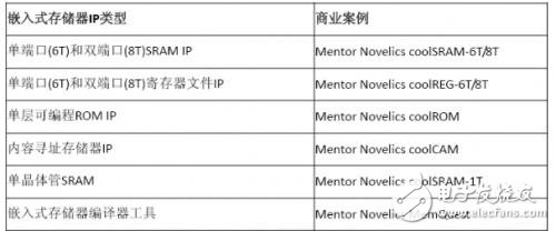
Table 2: Business case for embedded memory IP.
in conclusion
Choosing the optimal embedded memory IP for the new ASIC/SOC is the key to design decisions. Designers should be aware of all the key parameters that apply to the optimal memory characteristics of their particular application, and the memory IP they seek should be sufficiently adaptable to meet the various needs of the target SoC. Although ready-made free memory IP is available, it does not always provide the best solution compared to a paid IP that provides better features for a particular application.
The fully tuned memory IP features small size, low leakage power, low dynamic energy consumption, and fast speed, which allows the designer's solution to be further optimized to bring millions of dollars over the life of the product. The balance, but also its chips are better differentiated in the highly competitive ASIC/SOC market.
5050 Single Color Led Strip ,Single Color Led Strip,Single Color Led Strip Lights,Single Colour Led Strip
NINGBO SENTU ART AND CRAFT CO.,LTD. , https://www.lightworld-sentu.com