Realization of wireless communication system based on CDMA short message
In recent years, various application systems based on the SMS sending and receiving functions of the gsm module, such as stolen vehicle tracking systems and home network systems, have gradually become the focus of attention [1-3]. For these application systems, how to realize the function of sending and receiving short messages through the short message sending and receiving module is a very basic and very critical issue. With the continuous maturity of communication technology and the increasingly higher requirements of users for communication quality, the existing gsm network will inevitably evolve to w-cdma (Wideband Code Division Multiple Access). The cdma network has a wide coverage, low usage cost, perfect technology, safe and reliable. The short message service of the cdma network is used to realize wireless data transmission, which is convenient and reliable.
1 System design
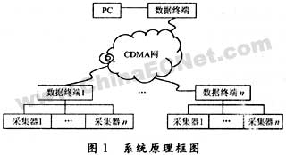
This system is mainly to use the short message service of the cdma mobile communication network to complete the wireless transmission of data, eliminating the initial construction cost of the on-site networking and future network maintenance costs. Through the data terminal, the collected field data will be sent to the monitoring center in the form of short messages, where the data processing, storage, and corresponding query, statistics, and report functions will be provided. The monitoring center can also update the real-time data of the data terminal by sending SMS to the data terminal, setting the monitoring terminal configuration information or control commands. The system consists of field devices, collectors, data terminals, and monitoring centers. The principle block diagram is shown in Figure 1.

2 Hardware design of data terminal
The data terminal uses cygnal c8051f020 as the main control chip. The chip has high integration and low power consumption (power supply voltage is 2.7 ~ 3.6v, typical operating current is 12ma, and has a variety of power-saving sleep and shutdown modes), strong processing capacity (Using the pipeline structure, the machine cycle is reduced from the standard 12 system clock cycles to 1 system clock cycle, and the peak performance can reach 25mips), making it very suitable for application in control systems that require high reliability and low power consumption . Cygnal c8051f is compatible: a single chip microcomputer with mcs-51 core, built-in 64kb flash program memory and 4352b data ram, with two full-duplex uart. It is the use of these two serial ports to achieve simultaneous communication between the microcontroller and the mobile phone module and pc. The block diagram of the hardware structure of the data terminal is shown in Figure 2.

2.1 Circuit design of communication unit
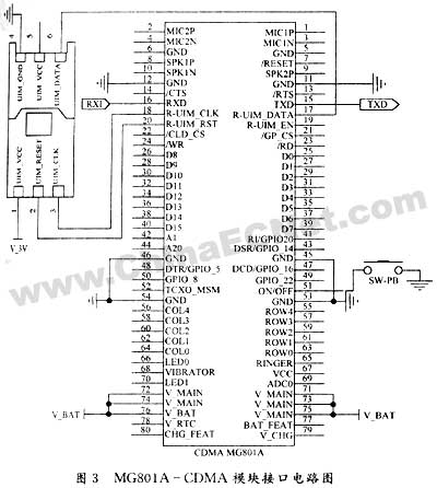
The communication unit is implemented by cdma wireless module. The cdma wireless module serves as the wireless transceiver module of the terminal, encodes the data information received by the single-chip microcomputer and sends it in the format of short message. The wireless module of cdma adopts the mg801a module of zteit. The mg801a-cdma module is an industrial-grade application module with built-in software supporting cdma2000 1x rev0 standard and gota protocol. The working frequency band is 800mhz. Can complete the functions of voice, data, fax, short message service and various additional services. It has the characteristics of large capacity, small radiation, low power consumption and small size. The module interfaces with peripheral circuits through an 80-pin socket. The circuit is shown in Figure 3. The power supply voltage of this module is 3.3 ~ 4.25v, the typical value is 3.8v.

2.1.1 On-off control
There are two ways to turn on the module, the first method is through the on / off pin on the system connector, and the second method is to use an external charger.
The 51st pin on the system connector is the on / off pin. Adding an instantaneous low level to this pin will turn on the module. The module is shut down by the at command. The shutdown command is at + zpwroff. The second method is to use an external charger to supply power to the module.If the external voltage is applied to v_main (pin 71, 72, 73, 74, 75) and vchg (pin 79) at the same time, the module will be turned on. When the charging power supply is removed , The module will shut down.
2.1.2 Communication
The mg801a module provides a serial asynchronous communication interface uart (the data communication between him and the serial port complies with the rs232 interface protocol). Because the single-chip microcomputer and the module are both about 3v power supply voltage, they all meet the ttl level standard, so they can be directly connected to achieve communication functions.
2.1.3 uim card
Uim card is a kind of smart card used by cdma mobile phone. The uim card provides personal authentication information and can allow ms or mobile phones to connect to the network. The uim card can allow users to make or receive calls and send and receive text messages. The uim card is fixed on the card socket, and is connected to the outside through the 6 pins of the card socket. In order to reduce power consumption, the mg801a module provides an enable pin for uim, which can be omitted here, so that the uim card is always in a working state.
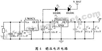
2.2 Regulated power supply circuit
The operating voltage of the data terminal is 5 v dc. In addition, not only the voltage requirements of the power supply, but also the power tolerance and other indicators must meet the requirements. Therefore, the design scheme of FIG. 4 is adopted. In this system, the switching power supply chip lm7805 completes the conversion from 12v to 5v, and two diodes are added to act as a step-down protection to supply power to the module. The power supply circuit is mainly composed of two three-terminal regulated power supply modules lm7805 and as117-3.o. The power supply module as117-3.o receives the 5v voltage input by lm7805 and outputs the 3v power supply voltage for the entire microcontroller system and uim card. The output of the power supply is basically not disturbed by external input changes, and the electromagnetic interference is effectively eliminated.
2.3 Single chip peripheral circuit
The single chip microcomputer adopts c8051f020 with dual serial ports of cygnal company, on the one hand, it realizes the initialization and control of the wireless module, on the other hand, it realizes the communication with the standard rs232 serial port. Need to explain is to add a level conversion circuit to convert ttl level to rs232 level, the sp3223 chip is used in this design. The function and performance of the c8051f020 single chip microcomputer have been greatly improved compared with the previous traditional single chip microcomputer, but the reset and clock circuits are no different from the previous single chip microcomputer. The jtag interface is added to enable online download and debugging functions underneath, thus making the entire development process simple and reliable.

3 System software design and implementation
The design of the system software lies in the programming of the single chip microcomputer. It sends different at commands to the mg801a module to achieve different functions, such as reading the content of the short message, deleting the short message, and listing the short messages that have not been read in the module. The following mainly introduces the realization of simultaneous communication of at command and dual serial port CPU.
3.1 at instruction
The at (attenTIon) command was originally launched by Hayes, which was mainly used to control the modem. It has now evolved into a standard, and all mobile modules support the at command. Although the mobile phone modules of different manufacturers all refer to the gsm protocol, the format is still different, and the data given by the manufacturers must be carefully consulted during the development process. At the same time, during the development process, it was found that the execution of instructions requires the completion of the interactive response between the microcontroller and the mobile phone. Each time the number of bytes sent or received has strict regulations, the two must implement data exchange in accordance with these regulations, otherwise, the communication fails. After repeated tests on several mobile phone modules, the author summarizes some rules. The following is a description of several issues:
All the instruction symbols, constants, pdu data packets of the at instruction are transmitted in the form of ascâ…± encoding. For example, the ascâ…± of "a" is encoded as 41h, the ascâ…± of "t" is encoded as 54h, and the ascâ…± of "o" is encoded as 30h Wait.
The single-chip computer controls the work of the mobile phone. If you want to send Chinese text messages, the gsm module must be used to set the short message work mode to pdu format, which is completed by the command at + cmgf = 0. Use mg801a module must be set to Chinese unicode code format, that is completed by at + zmsgl = 6,4.
After the MCU sends an instruction to the mobile phone, the carriage return character must be used as the end of the instruction.The ascâ…± code of the carriage return is odh.The carriage return character indicates the end of the instruction.If there is no carriage return character, the mobile phone will not recognize this instruction. instruction.
When the mobile phone receives a complete at command, the mobile phone does not immediately execute this command, but: first send all the asc â…± coding sequence of the at command just received back (including odh); secondly send a carriage return The asc â…± encoding of characters and line breaks, ie odh and oah; the instruction is executed last.
3.2 Realization of simultaneous communication of dual serial ports of single chip microcomputer
Because the c8051f020 microcontroller realizes simultaneous communication with the host computer and the mobile phone module, a CPU with dual serial ports is used. The CPU has 2 serial ports and 2 serial port interrupts. Serial port 1 interrupts processing communication with the host computer, and serial port 2 interrupts processing and For the communication of the mobile phone module, the serial port 1 interrupt is set to a high-priority interrupt.Each byte received or sent is interrupted, and the interrupt is immediately exited after processing.The communication baud rate is 115 200 b / s, 1 A start bit and a stop bit.
The programming language is c51, and modular, structured, and object-oriented programming is used as much as possible to make the serial communication program and other programs, and the two serial communication programs independent of each other, to reduce the chance of errors. In addition, in the serial communication, it is necessary to increase the communication timeout processing mechanism, pay attention to the protection of data and program status in the interrupt processing, and improve the error processing program. At the same time to solve the problem of time conflict, the time for a hardware to receive or send a byte is very different from the time for a software to receive or send a byte, which provides the conditions for simultaneous communication of dual serial ports. Secondly, to solve the problem of data conflicts, the two serial port communications use their respective receive and send data buffers and control variables to reduce the amount of interruption protection data and prevent data conflicts. When the main program, serial port 2 interrupt handler and other interrupt handlers write data to the memory (memory for communication with the host computer), the serial port 1 interrupt needs to be closed in the shortest possible time, and the closing interrupt time should be less than a few μs, Prevent serial port 1 from reading this data before writing other program data.
4 Conclusion
With the advancement of communication technology, microelectronics technology and the development of intelligent construction, more and more devices, such as home appliances, electricity meters, industrial terminals, etc., have the need for networking, and a large amount of data needs to be transmitted; and in In many cases, the way of wired connection can no longer meet people's needs. With its advantages of convenience, speed and cheapness, wireless access makes up for the deficiencies of wired methods. The cdma network covering the whole country has become a resource for sustainable utilization and development, so on this basis, it has become possible to use cdma's short message service to develop wireless access products that meet the needs.
Plug-in Terminal Block
It is made of two parts of plug-in connection. One part compresses the wire and then plugs it into the other part, which is welded to PCB. The mechanical principle of the connection bottom and the anti vibration design ensure the long-term airtight connection of the product and the use reliability of the finished product. The two ends of the socket can be equipped with lugs, which can protect the lug to a large extent and prevent the poor arrangement of the lug.
At the same time, this kind of socket design can ensure that the socket can be inserted into the matrix correctly.
The socket can also have assembly and locking positions. The assembly buckle can play a more stable role in fixing to the PCB, and the lock buckle can lock the mother body and the socket after the installation. Various socket designs can be matched with different insertion methods of the parent, such as: horizontal, vertical or inclined to printed circuit board, etc., and different ways can be selected according to the requirements of customers. Either metric wire gauge or standard wire gauge can be selected, which is the most popular terminal type in the market at present.
Plug-in Terminal Block
ShenZhen Antenk Electronics Co,Ltd , https://www.pcbsocket.com