Shanghai World Expo 38 enterprise investment to create LED cube
The Shanghai Enterprise Joint Pavilion of the 2010 Shanghai World Expo signed an official participation contract with the Expo Bureau on December 14. The museum was jointly funded by 38 large and medium-sized enterprises under the Shanghai State-owned Assets Supervision and Administration Commission. The funds are now in place. Because it is an ecological building with intelligent technology, dreamy mood and interactive experience, the Shanghai Enterprise Joint Pavilion is nicknamed Rubik's Cube.
It is understood that the architectural design of the Shanghai Enterprise Pavilion is inspired by the traditional Chinese Taoist thoughts of Tiandi and the romantic story of Zhuang Zhou Mengdie. The whole exhibition experience will be divided into Jingying Shenyin, into Pujiang, Shanghai Road and future journey. In the four areas, visitors will enter the pavilion and will travel with a dialogue between a grandfather and granddaughter. The integrated interactive experience lasts for 17 minutes.
The Shanghai Enterprise Pavilion covers an area of ​​about 4,000 square meters. Its façade material is made of polycarbonate transparent plastic tube, which is easy to recycle. The rainwater in the site will be recycled, precipitated, filtered and stored. Spray can not only reduce the local temperature, but also control according to the program, forming a colorful pattern on the building facade together with the LED lights. Interestingly, the Shanghai Enterprise Joint Pavilion has a solar collector screen on the roof of the building, and the output electric power is more than 200 kW, which can meet the daily electricity consumption and exhibition needs of the Rubik's Cube.
[ China's hotel lighting market is booming]
[ visualterrain lighting design case]
[ Hot discussion: The financial crisis that no one can escape? ]
[TracePro Coupling Selection Lamp Tutorial]
[ Wang Hao: IDDI Lighting Design Landed in Tianjin]
[Recommended: Chengdu Feixiang Lighting Design Studio]
1

Standard PCB
A Printed Circuit Board (PCB) mechanically supports and electrically connects electronic components using conductive tracks, pads and other features etched from copper sheets laminated onto a non-conductive substrate. Components (e.g. capacitors, resistors or active devices) are generally soldered on the PCB. Advanced PCBs may contain components embedded in the substrate.
PCBs can be single sided (one copper layer), double sided (two copper layers) or multi-layer (outer and inner layers). Conductors on different layers are connected with vias. Multi-layer PCBs allow for much higher component density.
FR-4 glass epoxy is the primary insulating substrate. A basic building block of the PCB is an FR-4 panel with a thin layer of copper foil laminated to one or both sides. In multi-layer boards multiple layers of material are laminated together.
Printed Circuit Boards are used in all but the simplest electronic products. Alternatives to PCBs include wire wrap and point-to-point construction. PCBs require the additional design effort to lay out the circuit, but manufacturing and assembly can be automated. Manufacturing circuits with PCBs is cheaper and faster than with other wiring methods as components are mounted and wired with one single part.
Here at BentePCB, Standard PCB means manufacture parameter in General requirements, no special features.
Parameter Definition of Standard PCB as below:
|
Items |
Manufacturing Capabilities |
|
Number of Layers |
1-16 layers |
|
Material |
FR-4 |
|
Maximum PCB Size(Dimension) |
650x1200 mm |
|
Board Size Tolerance(Outline) |
±0.2mm/±0.5mm |
|
Board Thickness |
0.8-1.6mm |
|
Board Thickness Tolerance(t≥1.0mm) |
±10% |
|
Board Thickness Tolerance(t<1.0mm) |
±0.1mm |
|
Min Trace |
0.1mm/4mil |
|
Min Spacing |
|
|
Copper Thickness |
1oz(35μm) |
|
Drill Sizes (CNC) |
0.3-6.3mm |
|
Min Width of Annular Ring |
0.15mm(6mil) |
|
Finished Hole Diameter (CNC) |
0.3mm-6.2mm |
|
Finished Hole Size Tolerance(CNC) |
±0.08mm |
|
Solder Mask |
LPI |
|
Minimum Character Width(Legend) |
0.15mm |
|
Minimum Character Height (Legend) |
0.8mm |
|
Character Width to Height Ratio (Legend) |
1:05 |
|
Minimum Diameter of Plated Half Holes |
0.6mm |
|
Surface Finishing |
HASL with lead |
|
Solder Mask |
HASL lead free |
|
Immersion gold |
|
|
Green ,Red, Yellow, Blue, White ,Black |
|
|
Silkscreen |
White, Black, None |
|
Panelization |
V-scoring, |
|
|
Tab-routing, |
|
Tab-routing with Perforation (Stamp Holes) |
|
|
|
About Us:
BentePCB is a professional PCB manufacturing which is focus on double side, multilayer, HDI PCB , rigid PCB and Flexible PCB mass production. The company was established on 2011.
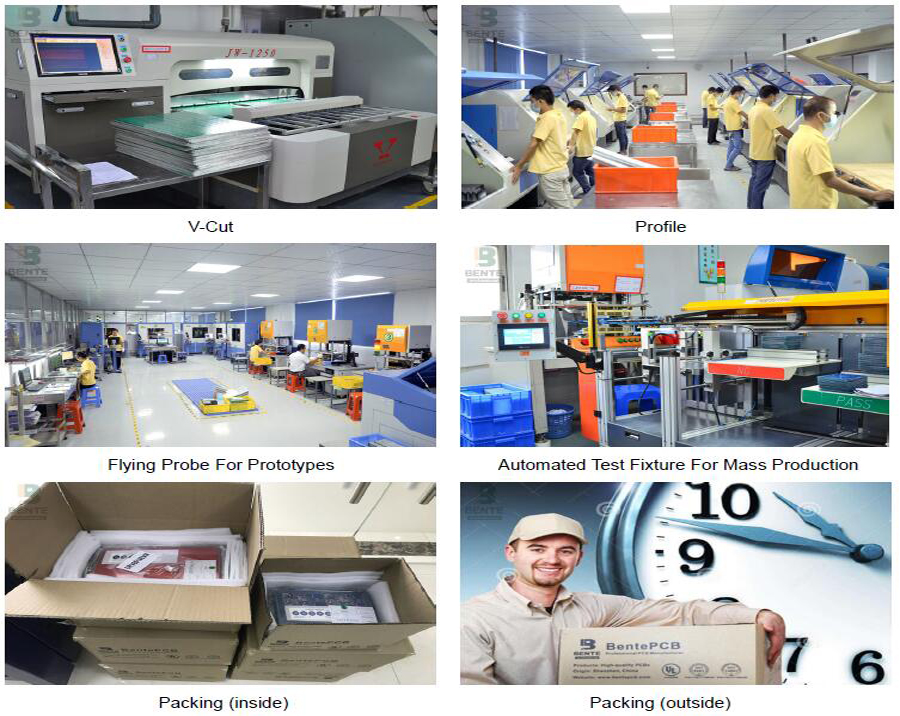
We have two factories together, The factory in Shenzhen is specialized in small and middle volume orders and the factory in Jiangxi is for big volume.
Why Us?
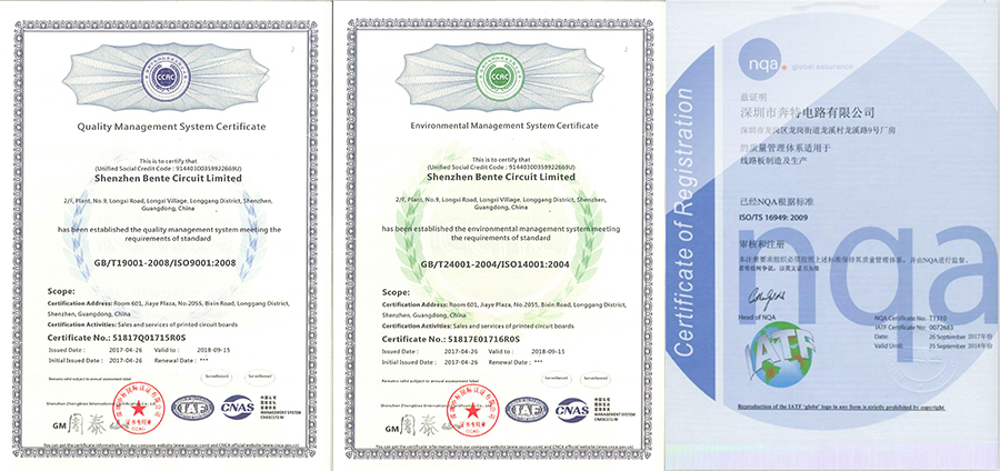
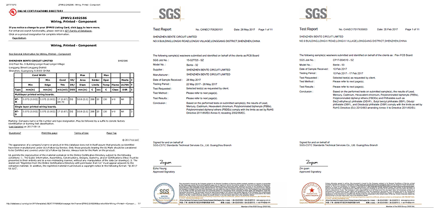
UL (E492586), ISO9001, ISO14001, TS16949, RoHS certified.
Turnover USD 10-50 million per year.
15,000 sqm area, 450 staff .
Mass Production from single to 16 layers.
Special Material:ROGERS, Arlon, Taconic.etc.
Client:Huawei, SAMSUNG, Malata, Midea,Texas Instruments.etc.
Certification(UL:E492586, TS16949, ISO14001, ISO9001,RoHS):
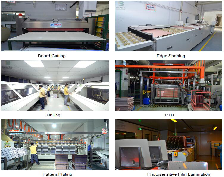
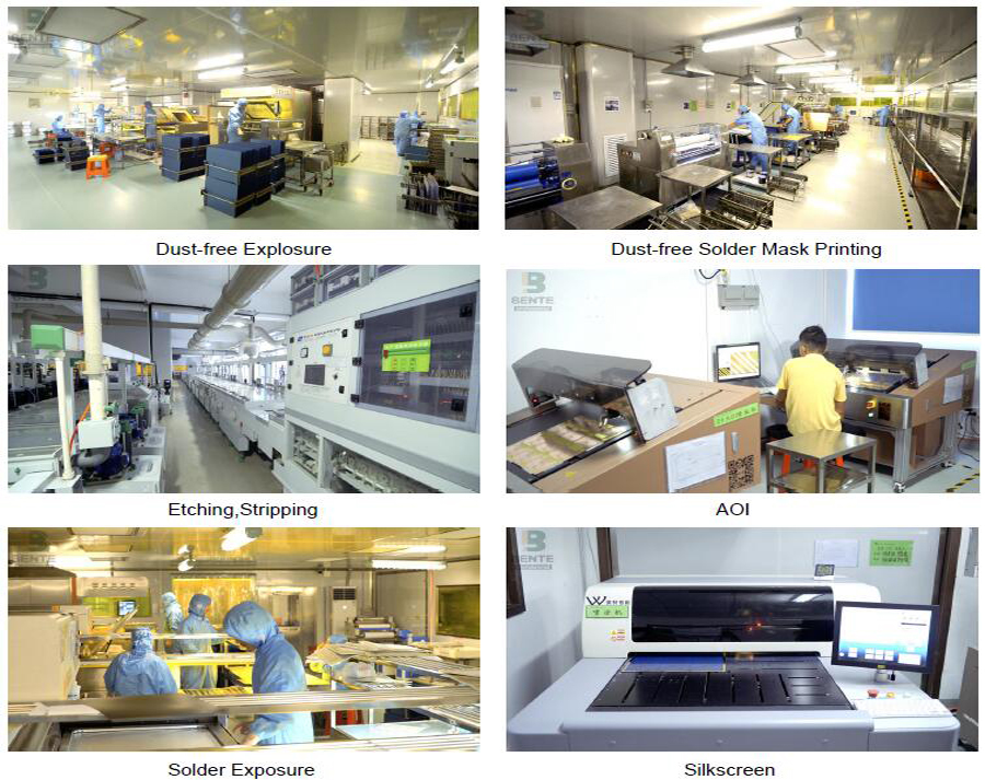
Factory Tour:
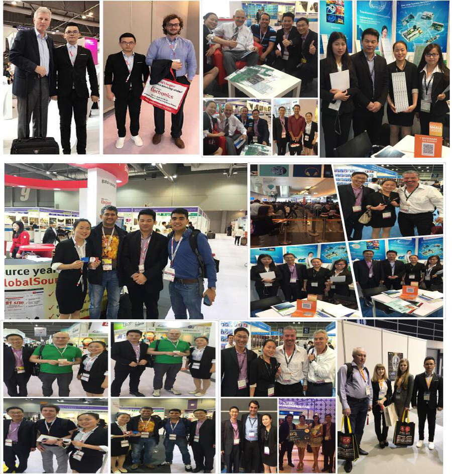
Exhibition:
We Took part in the famous exhibitions over the past years,and got highly appreciation from the top experts,as well as cooperated tightly with them.
Delivery:
BentePCB offers flexible shipping methods for our customers, you may choose from one of the methods below.


We don`t just sell PCBs .We sell sleep.

Standard PCB
Standard PCB, Printed Circuit Board, Circuit Board, PCB Circuit Board
Shenzhen Bente Circuit Limited , http://www.bentegroup.com