RFID (RadioFrequeryIdenTIficaTIon) radio frequency identification is a non-contact automatic identification technology. It automatically identifies target objects and obtains relevant data through radio frequency signals. The identification work can work in various harsh environments without manual intervention. The radio frequency identification system is mainly composed of a reader and an electronic tag. The data is stored in the electronic tag. When the electronic tag enters the effective range of the reader, both parties can communicate according to a certain protocol. RFID technology can identify high-speed moving objects and can identify multiple labels at the same time, and the operation is quick and easy. Short-range RF products are not afraid of harsh environments such as oil stains and dust pollution. Barcodes can be used in such environments, for example, to track objects on the factory's assembly line. Long-range radio frequency products are mostly used for traffic, and the recognition distance can reach several tens of meters, such as automatic charging or identification of vehicle identities [6]. In addition, because this technology is difficult to be counterfeited and invaded, electronic tags have extremely high security protection capabilities. The application of RFID is very extensive. At present, there are typical applications of animal chips and car chips. , access control, parking control, production line automation, material management. All countries and relevant international organizations are actively promoting the development of RFID technology standards. At present, there are not yet complete international and domestic standards for RFID. At present, the main RFID related specifications include the European and American EPC specifications, the Japanese UID (UbiquitousID) specification, and the ISO 18000 series of standards.
There are many kinds of RFID tags, and there are various classification methods. In accordance with the power supply can be divided into active and passive electronic tags; according to the carrier frequency can be divided into low frequency (134.2kHz), high frequency (13.56MHz), UHF (433MHz and 915MHz), and microwave electronic tags (2.45GHz The above) [6]; RFID single tag technology has matured, but there are still a lot of technical problems in the practical application of logistics or manufacturing. Such as: economy, signal interference, increase in recognition rate, information security and privacy protection, standardization and other issues.
The basic RFID system consists of RFID tags, RFID readers, and application support software. The CC2430 chip is supported by a powerful integrated development environment. The internal line's interactive debugging is supported by the IDE's IAR industry standard, which is highly recognized by embedded institutions. It also applies to 2.4 GHz frequency devices. The CC2430 chip is fabricated on an O.18μm CMOS process and consumes 27 mA of current during operation. In both receive and transmit modes, the current consumption is less than 27 mA or 25 mA, respectively. Available in 7mm & TImes; 7mm QLP package, a total of 48 pins. All pins can be divided into I/O port line pins, power line pins and control line pins [5]. The CC2430's sleep mode and ultra-short time transition to active mode are ideal for applications that require very long battery life. Especially suitable for the design of RFID systems. This article uses TI's CC2430 as the core to design active RFID tags. Use 3. 3-4. 5V. Can use button battery power, the chip power consumption is low. There are few peripheral circuits required, and all high-frequency components are integrated in the chip. Their operating performance is stable and free from external influences. Ideal for low power, high performance requirements of the application environment.
2. Label hardware design2.1 Hardware Circuit Structure
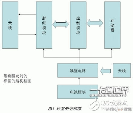
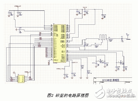
A typical active RFID tag is composed of an antenna, a radio frequency module, a control module, a memory, a wake-up circuit, a battery module, and the like as shown in FIG. The RF module completes the modulation and demodulation of the control signal and the response signal between the tag and the reader. The controller executes the reader's instructions. Memory stores tag related information and the microcontroller control program. The controller reads and writes memory. The radio frequency module includes a transmitting portion and a receiving portion. The transmitter includes modulators, power amplifiers, band-pass filters, mixers and local oscillators. The receiving part consists of a low-noise amplifier, a band-pass filter, a demodulator, and a detection shaping. TI's CC2430 chip integrates all of the wireless communication systems. It requires only a few external circuits to make it a wireless communication module, which reduces system costs and simplifies tag design. The CC2430 chip uses O. The 18μm CMOS process produces a current consumption of 27 mA. In receive and transmit modes, the current loss is less than 27mA or 25 mA, respectively. Available in 7 mm x 7 mm QLP packages with a total of 48 feet. All pins can be divided into I/O port line pins, power line pins and control line pins. The CC2430's sleep mode and ultra-short time transition to active mode are ideal for applications that require very long battery life. Especially suitable for the design of RFID systems. This tag is designed with a matching circuit to match the output to a 50 ohm microstrip patch antenna. All surface mount components are used in PCB design, which simplifies the complexity of the system and the size of the tags. The entire PCB is controlled within 10CM*5CM, which satisfies the miniaturization design of the tag. The circuit diagram of the tag is shown in Figure 2.
2.2 Low Power Design of Tags
For active tags, because of their use of battery power, the limited working life of the tags requires that the tags be energy efficient and their power consumption be low. This saves battery power and extends the working life of the tag. The CC2430 chip uses O. The 18μm CMOS process produces a current consumption of 27 mA. In receive and transmit modes, the current loss is less than 27mA or 25 mA, respectively. Adding a certain control program during the label design process can make the label enter the working state only in response to the reader's query request within the working range of the reader/writer. This maximizes energy savings.
2.3 Reader Design
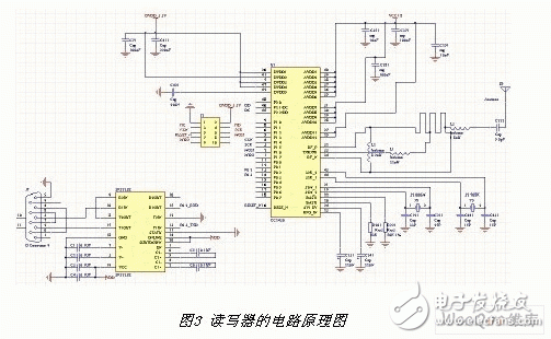
The reader is connected to the computer application network. We use serial communication. Its maximum transmission distance is 30 meters. The communication rate is generally lower than 20kbps [7]. Since most serial ports on MCU computers are RS-232C standard 9-pin interface. The MCU's pin input/output uses TTL level, and the short transmission quality is poor. Therefore, we need to convert these two different levels to achieve the correct communication between the reader and the computer. The reader's circuit diagram is shown in Figure 3.
3.1 register settings
The important parameters of the RF part of the chip, such as: receiving address, receiving and sending frequency, wireless transmission rate, transceiver mode, etc., must be set in its corresponding register configuration word. Correctly setting these parameters can increase the efficiency and reliability of the label.
3.2 Label workflow
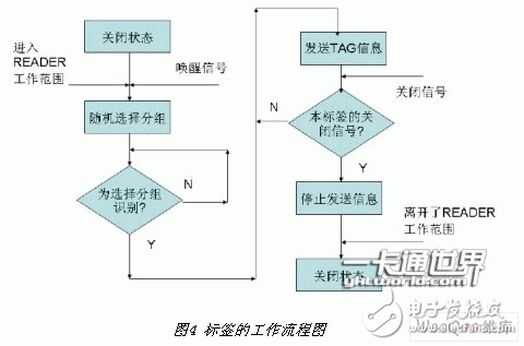
The label is normally in the power-off state when the label enters the work area of ​​the reader. The power of the wake-up signal causes the power comparator to output a high-level activation flip-flop to control the power supply chip to power the main circuit. In this way, the tag controller reads the information of the tag from the memory at the appropriate time according to the anti-collision algorithm program, and then modulates it through the RF module and amplifies the signal through the antenna. When the reader correctly identifies the tag, it will send the closing signal of the tag. After the tag is received, it is judged. If the tag is a close signal, the tag will no longer send information to the reader. When the tag leaves the reader's working range. The trigger controls the power switch chip to de-energize the tag's main operating circuit. In order to achieve the purpose of energy saving. The workflow of the label is shown in Figure 4.
3.3 Computer-side software design
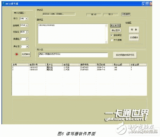
The software interface designed by the computer terminal is shown in the figure. It consists of a serial port setting area, a communication status area, a receiving and sending area, and an ID information display area. When the tag receives the reader's request, it sends its own information to the reader, receives the reader through the antenna and processes the information accordingly, and sends it to the computer through the serial port. The computer queries the database for the appropriate information to process. The corresponding information is displayed on the software interface as shown in Figure 5.
Right Angle D-sub Connector IP66 IP67 Rated
IP66 / IP67 waterproof d-sub connectors-Designed for IP Performance
ANTENK has developed IP66 / IP67 waterproof d-sub connectors that utilize a proprietary sealing technology, which maintains the same physical size and footprint as standard d-sub products.
Antenk's line of Waterproof d-sub connectors utilize an innovative sealing technology eliminating the need to redesign enclosures and PC boards when implementing IP67 design upgrades.These connectors are designed for applications that require protection from heavy spray or are exposed to short-term submersion. Connectors are available in vertical and right angle board mount types as well as solder cup for panel mount cable applications. Standard D-Subs are available in 9 pin, 15 pin, and 25 pin positions, and high density D-Subs are available in 15 pin, 26 pin, and 44 pin positions
Applications of Antenk waterproof d-sub connectors:
Hand held computers, scanners, and printers that are used outdoors
Remote sensors, gauges, and data loggers that are used outdoors
Industrial and Medical equipment that is routinely subject to wash down
Transmitters and emergency beacons that are subject to temporary submersion
Gas, Electric, and Water metering systems that have embedded Smart Grid electronics
Portable electric generation equipment (Gen Sets)
Consumer and Commercial boating electronics (Radios, Scanners, Radar, DC Power Ports)
IP67 D-SUB | WATERPROOF CONNECTORS FEATURES & BENEFITS
Signal / Low Power in 6 standard size
(Standard: 9 pin, 15 pin, 25 pin; High Density: 15 pin, 26 pin,44 pin)
Combo-D / High Power in a variety of configurations:
(3W3, 5W5, 7W2, 9W4, 11W1, 13W3, 13W6, 17W2, 21W1, 21WA4)
Solder Cup, Vertical Mount & Right Angle Board Mount Options
High Reliability Screw Machined Contacts
3 amp / 5 amp / 20 amp / 40 amp Power Options
-65°C to +105°C Operating Temperature Range
Right Angle D-SUB Connector IP66 IP67 Rated available in
3 industry sizes/positions:Standard Density (9 pin, 15 pin, 25 pin).
Male & Female Versions
Right Angle D-sub Connector IP66 IP67 Materials
Shell: Steel with Nickel Plating.
Insulator: Glass-filled thermoplastic. U.L. rated 94V-O
(260° process temp for board applications)
Machined Contacts:
Male Pins - Brass
Plating: Gold Flash on entire contact.
IP67 Right Angle D-Sub Seal: Proprietary Information
Right Angle D-Sub IP67 Rated,Right Angle D-Sub Waterproof,Standard Density Waterproof Right Angle D-Sub Connector, High Density Waterproof Right Angle D-Sub Connector
ShenZhen Antenk Electronics Co,Ltd , https://www.atkconnectors.com