Have you noticed the impact of the power supply on your RF system? For high-performance wireless communication systems, the impact of power on RF can be "hidden", but it cannot be ignored. Here, I collected and sorted out some key points and experiences in designing RF circuit power that are widely concerned in the industry.
(1) The power line is an important way for EMI to enter and exit the circuit. Through the power line, external interference can be transmitted to the internal circuit, affecting the RF circuit specifications. In order to reduce electromagnetic radiation and coupling, the primary side, secondary side, and load side loop areas of the DC-DC module are required to be the smallest. Regardless of the complexity of the power supply circuit, its large current loop should be as small as possible. The power and ground wires are always placed very close together.
(2) If a switching power supply is used in the circuit, the peripheral device layout of the switching power supply should conform to the principle of the shortest power return path. The filter capacitor should be close to the relevant pin of the switching power supply. Use a common mode inductor close to the switching power supply module.
(3) The long-distance power line on the board cannot approach or pass through the output and input terminals of the cascode amplifier (gain greater than 45dB) at the same time. Avoid the power line becoming an RF signal transmission path, which may cause self-excitation or reduce sector isolation. High-frequency filter capacitors need to be added to both ends of the long-distance power line, and even high-frequency filter capacitors are added in the middle.
(4) The three filter capacitors are connected in parallel at the power inlet of the RF PCB. The advantages of these three capacitors are used to filter out the low, medium and high frequencies on the power line. For example: 10uf, 0.1uf, 100pf. And in order from the largest to the smallest, close to the input pin of the power supply.
(5) Feeding the small signal cascade amplifier with the same set of power supply, starting from the final stage, and then supplying power to the previous stage, so that the EMI generated by the final stage circuit has less influence on the previous stage. And each stage of the power supply filter has at least two capacitors: 0.1uf, 100pf. When the signal frequency is higher than 1 GHz, a 10 pf filter capacitor is added.
(6) Commonly used to low-power electronic filters, the filter capacitor should be close to the triode pin, and the high-frequency filter capacitor is closer to the pin. The triode has a lower cutoff frequency. If the triode in the electronic filter is a high frequency tube, it works in the amplification area, and the layout of the peripheral device is unreasonable, and high frequency oscillation is easily generated at the output end of the power supply. The same problem may exist with the linear regulator module because the feedback loop exists in the chip and the internal transistor operates in the amplification region. In the layout, the high-frequency filter capacitor is required to be close to the pin, reducing the distributed inductance and damaging the oscillation condition.
(7) The copper foil size of the POWER part of the PCB corresponds to the maximum current flowing through it, and the margin is considered (the general reference is 1A/mm line width).
(8) The input and output of the power cord cannot be crossed.
(9) Pay attention to power supply decoupling and filtering to prevent interference from different units through the power line. The power lines should be isolated from each other when the power is routed. The power line is isolated from other strong interference lines (such as CLK) by ground.
(10) The power supply wiring of the small signal amplifier needs ground copper and ground via isolation to avoid other EMI interference, which deteriorates the quality of the signal at this level.
(11) Different power supply layers should avoid overlapping in space. Mainly to reduce the interference between different power supplies, especially between power supplies with large voltage differences, the overlap of the power plane must be avoided, and the middle interval formation can be considered when it is difficult to avoid.
(12) PCB board layer distribution facilitates subsequent wiring processing. For a four-layer PCB board (a circuit board commonly used in WLAN), components and RF leads are placed on the top layer of the board in most applications, and the second layer is used. Systemically, the power section is placed on the third layer, and any signal line can be distributed on the fourth layer.
The use of a continuous ground plane layout in the second layer is necessary to establish an impedance-controlled RF signal path. It also facilitates the shortest possible ground loop and provides a high degree of electrical isolation for the first and third layers, resulting in two layers. The coupling between them is minimal. Of course, other board definitions can be used (especially when the board has a different number of layers), but the above structure is a proven example of success.

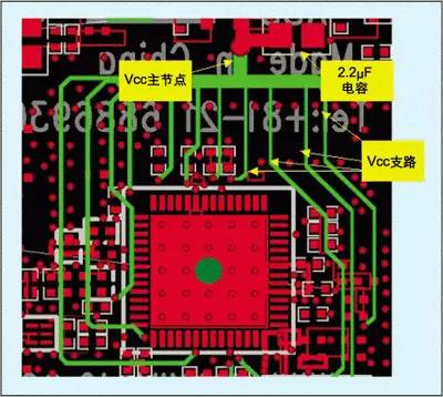
(13) A large power plane can make Vcc wiring easy, but this structure is often a fuse that causes system performance degradation. Connecting all power leads together on a large plane will not avoid pins. Noise transmission between. Conversely, using a star topology will reduce the coupling between different power pins.

The figure above shows the Vcc routing scheme for the star connection, taken from the evaluation board of the MAX2826 IEEE 802.11a/g transceiver. The figure establishes a main Vcc node from which the power lines of different branches are taken to power the RF IC's power pins. Each power pin uses a separate lead to provide spatial isolation between the pins, which helps to reduce the coupling between them. In addition, each lead also has a certain parasitic inductance, which is exactly what we want, it helps to filter out high frequency noise on the power line.
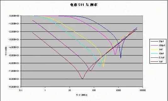
When using a star topology Vcc lead, it is necessary to take appropriate power supply decoupling, and the decoupling capacitor has a certain parasitic inductance. In fact, the capacitor is equivalent to a series RLC circuit, the capacitor plays a dominant role in the low frequency band, but at the self-oscillation frequency (SRF):

After that, the impedance of the capacitor will exhibit inductivity. It can be seen that the capacitors only have a decoupling effect when the frequency is close to or lower than their SRF, and the capacitance at these frequencies is low resistance.

Typical S11 parameters for different capacitance values ​​are given. SRF can be clearly seen from these curves. It can also be seen that the larger the capacitance, the better the decoupling performance provided at lower frequencies (the lower the impedance presented) .
It is best to place a large capacitor, such as 2.2μF, at the main node of the Vcc star topology. This capacitor has a low SRF and is effective for eliminating low frequency noise and establishing a stable DC voltage. Each power supply pin of the IC requires a low-capacitance capacitor (such as 10nF) to filter out high-frequency noise that may be coupled to the power line. For power supply pins that supply noise-sensitive circuits, two bypass capacitors may be required. For example, bypassing a 10pF capacitor in parallel with a 10nF capacitor provides decoupling over a wider frequency range, minimizing the effects of noise on the supply voltage. Each power supply pin needs to be carefully checked to determine how much decoupling capacitors are needed and at which frequencies the actual circuit is susceptible to noise.
The combination of good power supply decoupling technology with a rigorous PCB layout and Vcc leads (star topology) provides a solid foundation for any RF system design. Although there are other factors in the actual design that reduce system performance metrics, having a "noise-free" power supply is an essential element in optimizing system performance.
Our surface mount box could include the CAT5E CAT6 CAT6A RJ45 Connectors
The surface mount box is an ideal for wall box and wire installation, we design many junction box, back mount box, blank mount box, loaded surface mount box.
Mateiral: ABS, PBT UL94V-0
1~8 ports and colors supply for your choice, they are an ideal for low voltage application for your security, data, networking solutions and telecom projects.
blank surface mount box, junction box, surface mount box, loaded surface mount box in China supplier
NINGBO UONICORE ELECTRONICS CO., LTD , https://www.uniconmelectronics.com