Abstract: Based on a dedicated format conversion chip (VTP), a solution from SDTV to HDTV is proposed. The functional modules of this solution are analyzed, and the main characteristics of its circuit system are discussed. Finally, its application prospect is prospected.
For a long time, the video format conversion is mainly used for the conversion of ordinary analog TV and different TV systems. For example, the conversion between PAL and NTSC systems can meet the needs of different countries and TV systems in the international market. Until recently, with the advent of "100 Hz, progressive scan" TVs that used field or line frequency technology, most of the existing video format conversion technologies were still limited to the processing of analog TV signals. However, with the introduction and development of digital TV, in order to pursue higher definition, research and hardware implementation of digital video signal format conversion technology has gradually become a hot spot. After years of in-depth research and FPGA hardware verification [1], a digital video format conversion chip VTP (Video Transform Processor) finally successfully taped and passed the functional test.
The circuit system designed in this article is to provide a solution for this chip. The purpose is to input common standard definition digital signals, and after processing by this circuit, output the high-definition signals that can be received by digital high-definition televisions currently on the market to provide a A reliable source of programming. 
1 System structure and composition principle
Currently widely popular DVD players and satellite set-top boxes (STB), the processed video signals are generally based on MPEG-2MP @ ML encoding [2], and its image scanning format and ITU-RBT656 standard [3] required images Scan format compatible, namely 720x576x25 (PAL) or 720x480x30 (NTSC).
At the same time, due to the delay in the introduction of national standards for digital TV, various "digital high-definition televisions" that have been introduced in the market can only watch general programs without any meaning of "high-definition".
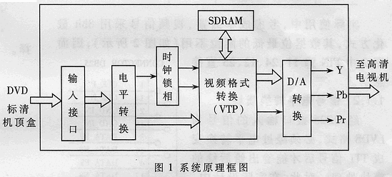
In this regard, combining the above two aspects and combining the functions of the VTP chip, a relatively inexpensive solution is designed. The basic block diagram is shown in Figure 1.
As can be seen from Figure 1, the input of the circuit system is a video signal (standard definition signal) that conforms to the ITU-RBT656 standard, and the output is an analog high-definition signal that can be played by high-definition televisions; in this circuit system, the standard definition video signal is completed to Conversion of high-definition video signals.
According to the video signal processing process in the circuit system, this circuit is divided into four modules: input interface module, clock phase-locked module, format conversion module and digital-to-analog conversion (D / A) module.
The following will analyze each module in detail.
1.1 Input interface module
In this module, it mainly includes two parts: input interface and level conversion to complete the preprocessing of the input signal.
1.1.1 Physical definition of input interface
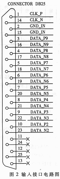
Since the input standard-definition video signal has a frequency of up to 27MHz, considering that the quality of the video signal must be guaranteed to reduce the interference received by the signal during the transmission process; differential signal transmission is required (LVDS signal is actually used), and then input into the circuit board Convert to ordinary TTL digital signal. According to the standard [3], the physical interface of the differential signal needs to be in the form of DB25.
In actual use, considering the cost factor, the video signal adopts 8-bit quantization, and the two lowest data bits are not used (as shown in Figure 2). Therefore, the PIN pins 11, 24, 12, and 25 in Figure 2 are directly suspended.
1.1.2 Signal level conversion module 
The signal input via the DB25 interface is in LVDS format, and it must be converted into a TTL signal after level conversion before being output to subsequent modules for processing. In this regard, in the actual design, the National Semiconductor (NS) special chip DS90LV032A is used to achieve the conversion of LVDS to TTL signals.
After passing through the interface module, the 8-bit video data and clock signal (27MHz) are actually output to the subsequent processing module; among them, the video data directly enters the format conversion module, and the clock signal enters the phase lock module to be converted into two phase-locked clock signals and then output To format conversion module.
1.2 Clock phase-locked module
For the format conversion module, the corresponding clock frequency of the input video data is 27MHz; and according to the SMPTE-274 standard [4], the high-definition digital television signal (1080i) sampling clock, that is, the corresponding clock of the high-definition data output by the VTP chip must It is 74.25MHz. Because the VTP chip does not contain the clock phase-locking function, it is necessary to provide two clocks with accurate phase lock input separately from the outside.
In this module, a dedicated video clock phase-locked chip is selected to achieve this function. The input clock passes the phase-locked circuit, and outputs two clocks, 27MHz and 74.25MHz, to the VTP chip to meet the needs of the internal SDTV and HDTV parts.
1.3 Video format conversion module
Video format conversion module is the core part of this circuit system, including VTP chip and SDRAM. The VTP chip is a dedicated video processing chip (ASIC), which has the following main functions:
· Up-conversion and Interlace to Progressive;
· Amplitude conversion (4: 3 to 16: 9);
· Any size zoom (ZOOM) and pan (PAN);
· Various format conversion (SD to HD, HD to HD, HD to SD).
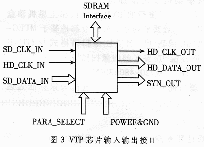
Its main input and output interfaces are shown in Figure 3:
· Input clock SD_CLK_IN (27MHz) and HD_CUK_IN (74.25MHz), the two are accurately locked in phase; input data 8bit (single channel) or 16bit (dual channel);
Output clock HD_CLK_OUT (74.25MHz); output data 16bit (8bit brightness signal, 8bit multiplexed color difference signal); output synchronization control signal SYN_OUT;
· SDRAM read and write interface;
· Parameter download interface PARA_SELECT is used to select the working mode.
This article only uses part of the functions of this VTP chip to complete the conversion from SDTV to HDTV. After being processed by the format conversion module, it outputs a digital high-definition signal in 16bit (4: 2: 2) 1920x1080i format.
1.4 Digital-to-analog conversion (D / A) module
After processing by the format conversion module, the output data is a 16-bit digital high-definition signal: brightness Y, multiplexed chrominance signal Cb, Cr; and the interface that the existing high-definition display can provide is analog high-definition signal input Y, Pb, Pr, Therefore, the signal must be digital-analog converted (D / A) before it can be output to the TV for playback.
In this module, the digital-to-analog conversion (D / A) chip uses Texas Instruments' dedicated high-definition digital-to-analog conversion chip THS8133, whose interface is compatible with SMPTE-274 and ITU-R BT656 standards, and internal three-channel digital-to-analog conversion It outputs three analog signals of Y, Pb and Pr at the same time. In this module, the digital-to-analog conversion of three video signals (one brightness and two chroma) can be completed with only one chip.
2 Some key issues
In the actual design, the circuit system studied in this paper solves a variety of technical problems, such as: there are multiple signals of different frequencies in the circuit, up to 27MHz (standard definition signal) and 74.25MHz (high definition signal); digital signal and analog signal Coexist in the circuit; even in the signal form there are TTL signal and LVDS signal. In the end, the author uses reasonable circuit layout, signal routing and ground division to ensure that this circuit system works reliably and stably. 
For this solution, because it is mainly aimed at the ordinary civilian market, cost reduction is the main factor considered in the design of this solution, and multiple solutions have also been adopted for this:
(1) Try to reduce the number of other non-core chips used in the circuit (for example, only one chip is used for the digital-to-analog conversion module), and strive to reduce the size of the circuit board, thereby reducing the cost of circuit manufacturing;
(2) Although the VTP chip has multiple functions, this circuit system does not verify its functional characteristics, so only some of the functions are used, that is, SDTV to HDTV (1080i) format conversion; because it is the default in the VTP chip Working mode, thus omitting the MCU module necessary for parameter download.
Due to the delay in the introduction of digital TV national standards, the high-definition terminal display market has begun to start due to the pressure of competition, resulting in such a strange phenomenon: various high-definition TVs can only watch ordinary TVs in practical applications program. The circuit solution studied in this article provides a cheap SDTV to HDTV solution, which directly outputs high-definition program sources from the end, thus solving the embarrassment of the existing high-definition televisions without high-definition programs.
Obviously, the solution of this paper will have a very broad application prospect before the introduction of digital TV national standards and the full realization of high-definition digitalization in the studio.

Follow WeChat

Download Audiophile APP

Follow the audiophile class
related suggestion