Abstract: Based on DALSA's CCD sensor FTT1010M, an image acquisition circuit for on-board CCD camera is designed and implemented. The characteristics, working mode and working timing of the image sensor FTT1010M are introduced in detail. The analog driving circuit and timing are also described. Design and implementation of image acquisition circuits such as circuits and power conversion circuits. After the actual project verification, the designed acquisition circuit can meet various technical requirements and has high practical value.
Key words: charge coupled device; image sensor; acquisition circuit; FTT1010M
0 Introduction Since the advent of CCD (Charge Coupled Device), it has been rapidly developed due to its high resolution, high sensitivity, low noise, small size, light weight, and high reliability. It has been widely used in image sensing. , satellite monitoring, space remote sensing imaging and Earth observation and many other fields. For a CCD camera system, the performance of the core device CCD sensor directly affects the performance of the entire camera system, and the design difficulty to ensure its excellent design lies in the design of high reliability drive, offset and other related to the image acquisition circuit. It brings a lot of trouble to the designer. Therefore, designing a stable and reliable CCD image acquisition circuit is an important condition to ensure that the CCD sensor and even the CCD camera system can perform their functions normally.
1 CCD camera image acquisition circuit structure CCD camera image acquisition circuit structure shown in Figure 1. The CCD sensor receives the imaging of the front end optical system, and the bias circuit provides the necessary bias voltage for the CCD sensor. The timing pulse generated by the programmable logic device controls the CCD through the driving circuit, and the output protection circuit can effectively protect the CCD. The pre-processing circuit processes the noisy analog signal outputted by the CCD to facilitate subsequent circuit use.
This article refers to the address: http://

2 CCD sensor selection CCD sensor is divided into area array CCD sensor and linear array CCD sensor. The linear array CCD requires less drive clocks, and the drive circuit design is relatively simple. The area array CCD requires more drive clocks, the timing is more complicated, and the drive circuit design is relatively difficult. Here we choose DALSA's frame transfer type array CCD1010M, because it has good radiation resistance design, it is an ideal image sensor in aviation and aerospace applications, and its resolution is 1024×1024, and it also has good anti-light. Halo performance, low signal output noise, large dynamic range, 100% optical filling efficiency, high charge transfer efficiency, etc., to meet project needs. Its multi-needle phase process (MPP) also ensures that it operates at low illumination and records very weak signals by extending the exposure time. The CCD has a four-phase sensitized area and memory cell electrodes, a three-phase horizontal readout shift register electrode, and an output amplifier. The output mode has two outputs and one output.
The single-channel output monochrome progressive scan image speed can reach 30 frames/s, and the dynamic range is greater than 72dB, and the performance is excellent.
2.1 FTT1010M structure The internal structure of the FTT1010M is shown in Figure 2.
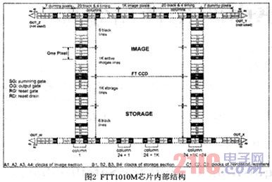
The FTT1010M is composed of a photosensitive area and a storage area, and both the photosensitive area and the storage area are composed of 1072H×1030V pixels. In the photosensitive region, each pixel unit can be regarded as a combination of four interconnected MOS capacitors covered by four-phase gate clocks A1, A2, A3, and A4 in the vertical direction, which serve as a photosensitive area frame transfer control clock. . There are six black lines (Black Lines) distributed on top of 1024 effective pixel rows. The black line is actually the shaded pixel row that does not participate in light integration; in the horizontal direction, the effective pixels in each row of 1072 pixels ( Active Pixels) is 1024, with 2×20 black pixels (Black Pixels) and 2×4 transition pixels (Overscan Pixels) on both sides. Black pixels are also shaded pixel units like black lines. These units do not participate in light. Integral, no photo-charge packet is generated, its main function is to reference the black level when pre-processing the output video signal of the CCD. The function of the transition pixel unit is mainly to play a transition between the effective pixel unit and the black pixel unit.
In the memory area, each pixel cell can be regarded as a common combination of four interconnected MOS capacitors covered by four-phase gate clocks B1, B2, B3, B4 in the vertical direction, which serve as a bank transfer clock. There are two serial output shift registers in the horizontal direction of the storage area. There is no photosensitive unit inside the register, only the transfer unit for transmitting the shadow of the transfer photosensitive charge package, each unit is equivalent to being three-phase. The clocks C1, C2, and C3 are covered, and these units are connected to the pixel units of the storage area. Its main function is to connect the output amplifier to the horizontal output shift register.
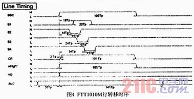
2.2 FTT1010M Timing Design The working timing of the FTT1010M image sensor can be divided into frame timing, line timing and Pixel timing. The frame transfer timing refers to the timing at which the CCD transfers the output of one frame of image. The line transfer timing refers to the timing at which a row of pixels is transferred from the storage area to the horizontal shift register under the driving of the clock. The pixel readout timing refers to the driving of the C clock in one row of pixels. The timing of horizontal readout from the horizontal shift register.
The working process of the FTT1010M can be divided into two phases: the photosensitive phase and the transfer phase. In the photosensitive phase, the image sensor senses the charge accumulation, the memory area performs the charge transfer to the horizontal shift register and the charge output of the horizontal shift register to the output amplifier; during the transfer phase, the image sensor mainly completes the accumulated charge by the photosensitive array. Transfer to the storage area. The frame timing of the FTT1010M is shown in Figure 3.
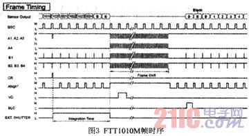
In the photosensitive phase, the photosensitive array generates electric charge under the illumination of the external light source. At this stage, the frame transfer control signals A1, A2, A3, and A4 do not change, and the photosensitive region and the storage region are in a blocking state, and the charge does not shift; At this stage, the memory area is in the row transfer state and the charge is output. The process of line transfer is divided into two stages: row forward and row reverse.
In the line reversal phase, SSC is at a high level, and the charge of each pixel unit in the storage area is shifted down to the horizontal shift register under the control of the row transfer signals B1, B2, B3, and B4, and the pixel transfer signals C1 and C2 are shifted. C3 does not change, and the image sensor has no pixel charge output. The FTT1010M line transfer timing is shown in Figure 4.
In the positive phase of the line, SSC is low, the row transfer signals B1, B2, B3, and B4 are not changed, and the pixel charges in the horizontal shift register are successively passed through the output amplifier under the control of the pixel transfer signals C1, C2, and C3. Output, after each line of signal output, a row transfer. The FTT1010M pixel readout timing is shown in Figure 5.

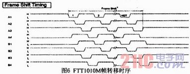
In the transfer phase, the frame transfer control signals A1, A2, A3, and A4 and the row transfer control signals B1, B2, B3, and B4 simultaneously act to overlap and change the charge accumulated in the photosensitive region to the storage area line by line. During the segment, the pixel transfer signals C1, C2, and C3 do not function, and the charge is not outputted outward. After completing the entire transfer phase, the photosensitive phase is again entered, and the cycle is repeated to ensure the operation of the image sensor. The FTT1010M frame transfer timing is shown in Figure 6.
3 CCD Bias Voltage Circuit To make the CCD image sensor chip work properly, it is necessary to provide the CCD with the bias voltage required for its normal operation. The bias voltages required for the FTT1010M are VNS, VPS, SFD, RD, OG, etc. Their parameters are shown in Figure 7. At the time of design, the voltage conversion scheme adopted by the author is to use a low-ripple conversion chip with a conversion circuit. VNS (24V) is obtained by an external 28V voltage through a DC/DC converter LT3060, and SFD is obtained by VNS through a level conversion circuit. VPS, RD and OG are extracted by the partial pressure of SFD.

4 CCD drive circuit The voltage of the various pulse signals required for the operation of the FTT1010M is shown in Figure 8.
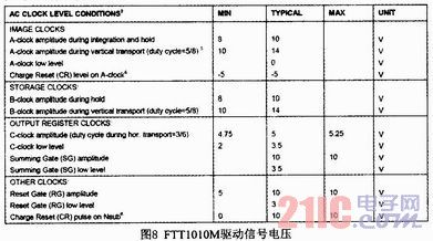
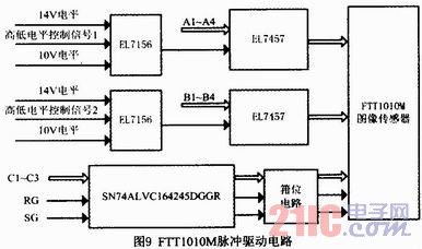
The lower level of the A and B drive clocks is 0V. As can be seen from Figure 8, in the photosensitive phase, the high level of the A and B drive clocks is +10V. In the transfer phase, the high level of the A and B drive clocks is +14V. Here I use EL7156 to achieve high-level conversion, EL7457 to achieve low-to-high level conversion.
The low level required for the horizontal readout clock C is not 0V but 3.5V, and the high level is 8.5V. The clock pulse given by the FPGA is a low level of zero and a high level of 3.3V. Therefore, the clock generated by the FPGA needs to be driven by the driving chip SN74ALVC164245DGGR to make the amplitude of the clock C reach 5V, and then the coupling of the clamping circuit is used to increase the pulse level, and the pulse is mentioned to the required amplitude.
The generation process of SG and RG is similar to the generation process of clock C, except that the amplitude requirement is 10V.
The amplitude adjustment circuit of various driving pulse signals is shown in FIG.
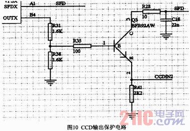
5 CCD output protection circuit CCD sensor is a kind of MOS device. It is easily damaged by static electricity when it is improperly operated. In the circuit design, clamp and current limiting circuit should be added to its peripheral circuit to ensure each offset applied to the CCD. The voltage and drive pulses are current protected and should be decoupled by a capacitor before being input to the FTT1010M, and the decoupling capacitors should be as close as possible to the image sensor pins. The output of the FT T1010M is an open source output. A current source should be connected to the output for load or a resistor to ground. Add an emitter-followed high-frequency transistor to the output to prevent the output from being limited by the capacitive load. In addition, the emitter follower is added to the output to prevent electrostatic damage to the FTT1010M from the oscilloscope's probe. The CCD output protection circuit is shown in Figure 10.
6 CCD output preprocessing circuit In CCD imaging systems, noise is the most important factor limiting the effective resolution. The signal output by the CCD is an analog signal with various noises, which must be pre-processed to eliminate noise and various interferences as much as possible for subsequent circuits. In order to facilitate computer processing, it is also necessary to perform A/D conversion on the signal output from the CCD. The pretreatment process is generally shown in Figure 11.

According to the requirements of pre-processing, we chose a highly integrated CCD signal processing chip AD9978, which has dual-channel output capability, 14-bit A/D conversion accuracy, conversion frequency up to 65MHz, and its internal integration Dual sampling, variable gain control, black level clamp circuitry, and high precision timing generation system. We use the correlated double-sampling processing unit to eliminate unwanted noise components by two samples. The first sample is located at the end of the reset period, and the second sample is located at the information segment of the signal. The difference between the two samples is the noise-free signal. . Subsequently, in order to adapt to different brightness targets, to prevent the CCD signal from being too weak or saturated, we use the gain control processing unit to control the gain of the signal, and finally send it to the following programmable logic unit for processing by A/D conversion. Also pay attention to the design of the conversion rate and the CCD output pixel clock.
7 Conclusion This paper describes the design and implementation of the image acquisition circuit of the on-board CCD camera. The project verification shows that these designs can provide various kinds of bias voltage, drive pulse and circuit protection for the CCD, which ensure the CCD image sensor. The image quality makes the CCD camera imaging system high performance and high reliability, and has extremely high application value.
Led Driver,Mini Led Driver,100W Led Driver,100W Led Driver
Ninghai Yingjiao Electrical Co., Ltd. , https://www.yingjiaoadapter.com