Abstract: This paper describes the general characteristics of the CMOS image sensor, the detailed properties, characteristics and working principle of monochrome CMOS image sensor chip of OV9120, OV9120 given specific application example of the image acquisition and processing.
1 Overview
With the development of CMOS technology and the increase in market demand, CMOS image sensors have developed rapidly. CMOS image sensor has the advantages of high integration, low cost, low power consumption, single operating voltage, local pixel programmable, random reading, etc. It is suitable for ultra-mini digital cameras, portable video phones, PC computer eyes, video doorbells , Scanners, cameras, security monitoring, car anti-theft, machine vision, car phones, fingerprint recognition, mobile phones and other image fields. This article is produced by the American company's technology OmniVision OV9120 monochrome CMOS image sensor, which uses a unique patented sensor technology and advanced algorithms (algorithms) to solve the previously fixed limits CMOS image noise sensitive device (the FPN) a. Therefore, it can be widely used in digital still camera, video conference, video telephony, computer vision, biometrics and other fields.
2 Pin function
OV9120 48-pin LCC package, the pin arrangement shown in Figure 1. 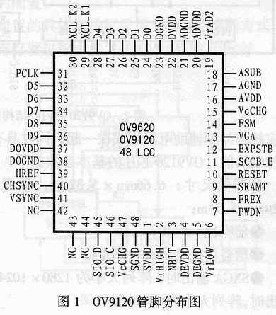
3 Structural performance and working principle
3.1 Internal structure
Built OV9120 resolution 1312 × 1036 image array of 10-bit A / D converter, the adjustable video window, SCCE interfaces, programmable frame rate control, programmable / auto exposure gain control, and external frame sync counter balanced luminance, digital Circuits such as video port, timing generator, black level calibration and white balance control. Its internal structure is shown in Figure 2.
3.2 Performance characteristics
OV9120 is a 13.5-megapixel (1312 × 1036), 1 / 2-inch CMOS image sensor chip, which uses the SXGA / VGA format, the maximum frame rate can reach 30 frames / s (VGA), the chip will CMOS light sensor core and The peripheral auxiliary circuits are integrated together and have programmable control functions. The basic parameters of the OV912 chip are as follows?
◠Image size: 6.66mm × 5.32mm, pixel size, 5.2μm × 5.2μm;
â— Signal-to-noise ratio> 54dB;
◠Gain adjustment range: 0 ~ 24dB;
◠When SXGA is output, the array size is 1280 × 1024, and when VGA is output, the array size is 640 × 480;
â— The power supply voltage is DC 3.3V and 2.5V;
â— Dark current: 28mV / s;
â— Dynamic Range: 60dB.
3.3 Working principle
The design of the CMOS mirror array is mainly based on the field-by-line scanning field readout system and the electronic shutter with synchronized pixel readout circuit. And an electronic exposure control algorithm (or system rules) is established throughout the drawings (object) image on the basis of brightness. When the scene (or scene) is normal, the general exposure is ideal. But when the scene light is not suitable, it should be adjusted by automatic exposure control (AEC) white / black ratio to meet the application requirements. For VGA format output, the window size of the OV91220 image sensor ranges from 2 × 2 to 640 × 480, while for SXGA format output, the window range is from 2 × 4 to 1280 × 1024, and it can be within the internal 1312 × 1036 boundary anywhere positioning. Changing the window size or position will not change the frame rate (or data rate). The frame rate can be changed by the master clock downstream, the insertion of vertical synchronization timing, or the QVGA format using skip read technology.
OV9120 embeds a 10-bit A / D converter, so it can output 10-bit digital video stream D [9. . 0]. While outputting digital video streams, it can also provide pixel synchronization clock PCLK, horizontal reference signal HREF and vertical synchronization signal VSYNC to facilitate external circuits to read images. 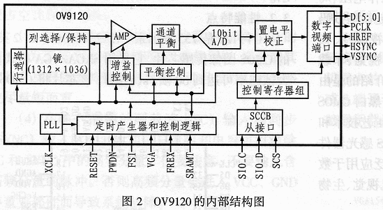
ZV port is the camera (lens) of focal length to adjust the video port. The ZV function of OV9120 can make the camera lens zoom and move quickly (or away) to the target. OV9120 can use external leading agencies (master device) to set the exposure time. When FREX is set to 1, the pixel array is quickly charged and the sensor remains high to take an image (or object image). When FREX is converted to 0, the video data stream (data stream) is delivered to the output port by line-by-line readout. When data is output from the OV912 video output, special care should be taken to prevent the image array exposure from affecting the integrity of the captured image data. An automatic shutter synchronized with the frame's exposure rate can minimize this effect.
When OV9120 the RESET pin pulled up to VCC, all the hardware reset. At the same time OV9120 will clear all registers and reset to their default values. In fact, the reset can also be triggered by the SCCB interface.
Since the SCCE port can access all the internal registers, the internal configuration of the OV912 can be performed through the SCCE serial control port. SCCB interface has SCCE, SIO_C, SIO_D three leads, wherein SCCE enable signal is a serial bus, a serial bus clock signal is SIO_C, SIO_D data signal is a serial bus. The control of the bus function by SCCB is completely dependent on the status of the three bus levels of SCCE, SIO_C, and SIO_D and the mutual cooperation between the three. Control bus predetermined conditions are as follows: When SCCE from high to low, the data transfer begins. When SCCE converted from low level to high level, the data transmission ends. In order to avoid the transmission of useless information bits, SIO_D can be set to a high level before the transmission starts and after the transmission ends. During the data transmission, SCCE always keeps low, at this time, the data transmission on SIO_D is controlled by SIO_C. When SIO_C is low, the data on SIO_D is valid, and SIO_D is in a stable data state. When every positive pulse appears on the IO_C, the system will transmit one bit of data.
OV9120 has two modes: master and slave modes. In the main mode, OV9120 is used as the leading device. At this time, the external crystal input on XCLK can get the PCB signal after the internal frequency division. After the image is collected by OV9120, when the falling edge of PCL comes, the system can output the pixel values ​​in sequence, and the outside is only passively receiving the signal. In slave mode, OV9120 can be used as a slave device. At this time, XCLK cannot be connected to an external crystal, but it can be controlled by external devices, that is, the signal of the master device. That is, a MCCK clock signal is sent by the leading device, and the pixel values ​​are sequentially sent under the synchronization of this signal.
4. Application of OV9120 in image acquisition system
The entire image acquisition system is mainly composed of OV9120 image sensor chip, CPLD control module, RAM memory, DSP signal processor, crystal oscillator circuit and other parts.
In this system, OV9120 as the image sensor of the system, firstly quantizes the acquired image within it, then outputs the digital image under the control of external logic and stores it in the image memory. As the main control module of the core control logic of the acquisition system, CPLD can be used to coordinate the work of other modules. The configuration of the SCCB bus parameters of OV912 is the starting point for the execution of the entire control logic module. Only after the configuration of OV912 using the SCCB bus can image acquisition work be performed. The image data acquired by OV9120 can be stored in SRAM for DSP to complete the interactive operation between the image acquisition system and the DSP recognition system. The system schematic diagram is shown in Figure 3.
After the system is powered on, it should first initialize the CMOS image acquisition chip to determine the window position, window size, and black and white working mode of the acquired image. These parameters are controlled by the corresponding register values ​​in OV912. Since the value of the internal register can be accessed through the SCCB serial control bus interface provided on the OV91220 chip, CPLD can complete the configuration of parameters by controlling the SCCB bus.
The specific method of configuration can use the three-phase data writing method, that is, in the process of writing the register, the ID address of OV912 is sent first, then the destination register address for writing data is sent, and then the data to be written. If you write data to a register continuously, then after writing a register, OV9120 will automatically add 1 to the register address, and then continue to write down under program control without entering the address again. 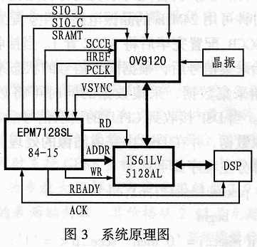 Three-phase write data becomes two-phase write data. Because the system only needs to change the data of a limited number of discrete registers, and configuring all the registers will waste a lot of time and resources, so only the registers that need to be changed can be written. For each changed register, the three-phase method of writing data is used.
After the system is configured, image data will be collected. In the process of collecting images, the most important thing is to determine the start and end time of a frame of image data. Based on a careful study of the OV9120 output synchronization signal (VSYNC is a vertical synchronization signal, HREF is a horizontal synchronization signal, and PCLK is an output data synchronization signal), accurate control of the starting point of the acquisition process can be achieved using VHDL language.
The rising edge of VSYNC indicates the arrival of a new image, and the falling edge indicates the start of image data acquisition for a frame (CMOS image sensors acquire images in columns). HREF is a horizontal synchronization signal, and its rising edge indicates the beginning of a column of image data. PCLK is the output data synchronization signal. HREF is high to begin effective data collection, and the arrival of the falling edge of PCLK indicates that the data generated, PCLK Every falling, the system will transmit one bit of data. When HREF is high, the system transmits a total of 1280 bits of data. That is to say: in a frame of image, that is, during the period when VSYNC is low, HREF will appear 1024 times high. The arrival of the next rising edge of the VSYNC signal indicates the end of the image acquisition process with a resolution of 1280 × 1024.
The software design for the acquisition can be implemented in the MAX + plusII environment. The main work of software design is the configuration of OV912 by CPLD. When starting charging, first initialize the system. The global clock of CPLD can be generated by a 24MHz crystal oscillator circuit. When configuring, configure the SCCB first, and set the SCCE to 1 after configuration. After receiving the DSP start acquisition signal, it is determined whether to start data collection according to the status of the synchronization signal, and the data can be sent to the SRAM while collecting data. When the DSP receives the CPLD read signal, it can start to read the data and complete the image processing in the DSP. Acquisition and processing of a main program as follows:
reset2: procedures (resset_i, n1, lock)
begin
ifreset_i = '0'then scene_p <=' 1 ';
else
if (n1 = '1' orm1 = '1') then
sce_p <= '1';
else scene p <= '0';
end if;
end if;
end provinces reset2;
clk1: procedures (n1, clk)
variable a: integer range 254 to 0;
begin
iff (sio_c_statt = '0' OR nn1 = '1') then
q < ï¼ '1'; a: ï¼ 0;
else
if (clk 'ever and an clk =' 1 ') then
iff (sio_c state = '1' and n1 = '0') then
if a <254 then; a: = a + 1;
Else a: = 1;
end if;
if a <127 then q <= '0';
else q < ï¼ '1'; end if;
end if;
end if;
end if;
end provinces lock1;
lok: process (sio_c_state, q)
variable n: integer ran 8 8 to 0;
begin
if (sio_c_statt = '0' then load <= '1'; n: = 0;
else
if (q ‘evend and and q =’ 0 ’) then
if n <8 then n = n + 1?;
load <= '0';
else n: = 0; load <= '1';
end IF;
end IF;
end if;
end procs lock;
leg1: procedures (n1, q, load)
variable pp: std_logic_vector (7 downto 0) ;?
variable b: internet rang 7 to 0;
variable c: internet rang 13 to 0;
begin
if (n1 = '1'or reset_i =' 0 ') then p <=' 1 '; c: = 0; b: = 0; QB <=' 0 ';
else
if (q'evend and q = '0') then
if load = '1' then;
c: = c + 1?
if c <13 then
if c = 1 then
pp: = "110000100";
elsif c = 2 then
pp: = "000011100";
elsif c = 3 then
pp: = "001010001";
elsif c = 4 then
pp? = "1100000";
elsif c = 5 then
pp: = "00001101";
elsif c = 6 then
pp: = "1000000";
elsif c = 7 then
pp: = "11000010";
elsif c = 8 then
pp: = "00001001";
elsif c = 9 then
pp: = "1000000";
elsif c = 10 then
pp: = "11000010";
elsif c = 11 then
pp: = "00010011";
elsif c = 12 then
pp: = "00010011"?
end IF;
b: = 0; p <= pp (7);
elsif c = 13 then
p <= '0'; QB <= '1';
end IF;
else
if b <7 then b: = b + 1;
pp (7 dowto 1): = pp (6 ownto 0);?
p <= pp (7) ;?
else p <= '1';
end IF;
end IF;
end IF;
end IF;
end process reg1;

Follow WeChat

Download Audiophile APP

Follow the audiophile class
related suggestion
X9511 is the ideal button type number
![[Photo] The principle and application of button digital potentiometer X9511](http://i.bosscdn.com/blog/20/06/41/7212119738.jpg)
![[Photo] The principle and application of single-chip switching power supply](http://i.bosscdn.com/blog/20/06/41/5232556415.jpg)
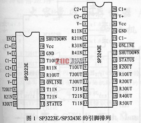
Abstract: SP3223E / 3243E is an RS-232 transceiver interface chip produced by SIPEX. The device contains ...
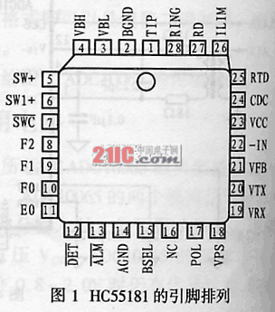
Abstract: HC55181 is a subscriber line interface circuit (SLI ...
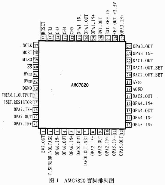
Abstract: AMC7820 is an analog monitoring and control circuit designed for multi-channel applications by Texas Instruments (TI). It contains ...
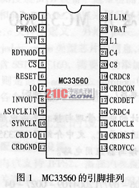
Abstract: MC33560 is a power management and interface integrated circuit designed by ON Semiconductor for smart card reader / writer applications. It passes ...
1 Main Features DS 2770 is a battery fuel gauge and lithium / produced by Dallas Semiconductor Corporation ...
