The semiconductor industry has come to a crossroads: some designs are pursuing a micron-to-nano-node process, but most designs still stay at 28-nm or older nodes.
Just as we predicted more than two years ago, the IC industry is developing separately, and only a few products are actively pursuing miniaturization to 7nm process nodes, but most of the designs still stay at 28nm or older nodes.
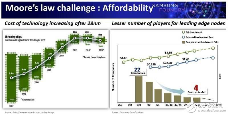
In an article published in 2014, the author pointed out that the last node of Moore's Law has confirmed that it is 28 nanometers; the article wrote: "After 28 nanometers, we can continue to make the transistor more Small, but not cheaper;" Samsung's briefing at the recent Semicon West 2016 conference as described below.

Intel also said that the evolution of semiconductor process nodes will be lengthened in the future, but the company claims that the cost of transistors can still continue to decline; but Intel has not made impressive achievements in the field of foundry, showing This is not the case.
In another blog post, the author mentioned: "Intel will claim that their 10nm and 7nm nodes are better than other foundries (such as TSMC and Samsung), but this requires PAAC at the wafer level. -- Power, performance, area, and cost -- as evidenced by the benchmark; at every process node, other foundry companies beat Intel at the SoC's PPAC. I don't expect this to change at 10 nm or 7 nm."
These discussions now seem to be too theoretical, but the actual engineering costs of advanced process node components have proven to be too expensive for most manufacturers in the industry; therefore, as predicted by the parties, the semiconductor industry has indeed developed separately, with only a few The pursuit of miniaturization to 7 nanometers, while most still maintain designs with 28 nanometers or older nodes.
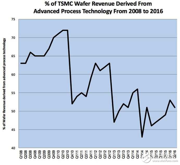
The picture below shows a change in the revenue of advanced process nodes from the TSMC earnings report quoted by Ed Sperling, a senior editor of the semiconductor industry, in a recent blog post; perhaps even more, The 50-year-old Moore's Law is really coming to an end, and the industry is now facing a new reality.

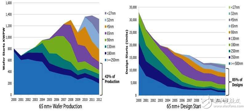
A similar trend observation comes from a blog post by an author of Mentor Graphics: “Process nodes at 65 nm and above still account for about 43% of total wafer production, or 48% of fab capacity; a clearer trend Yes, 65 nm and above occupy nearly 85% of all design starts (as shown below); apparently mature process nodes will still not retreat in a short period of time."

This is good news for innovation, as diverse choices help support new ideas and new technologies such as 3D NAND, FD-SOI, MEMS, etc., which can be implemented for emerging Internet of Things (IoT) applications. New product.
Compilation: Judith Cheng
(Reference: 28nm Was Last Node of Moore's Law, by Zvi Or-Bach; the author of this article is the founder of MonolithIC 3D)

"How can you miss this new feast of the Internet of Things?! The 3rd "China IoT Conference" organized by Huaqiang Jufeng's Electronic Enthusiasts Network will be held in Shenzhen on December 2: Global Vision The exclusive view of higher value, more professional technology sharing, more cutting-edge pulsation, gathering of the world's well-known enterprises and elites of the Internet of Things, you must not miss it! More information welcome everyone to continue to pay attention to the electronic enthusiast network!" (Click on the picture see details)
Educational Instrument;Student experimental equipment;laboratory training
Wuxi Lerin New Energy Technology Co.,Ltd. , https://www.lerin-tech.com