What are the biggest factors that affect the productivity of FPGA design cycles, tools, techniques, and methods to improve FPGA design productivity? The answer to many designers is that timing closure is the key to moving product design to market. Efficiently achieving timing closure and achieving credible results is the dream of every designer. However, this is only part of the problem.
To be truly efficient throughout the design cycle, designers need to rely on the entire design environment and the many tools involved to manage process complexity and provide a true solution to the unique style and approach of FPGA design. A complete and effective design environment provides the focus and transparency of the problem, and it is best to provide a seamless solution.
To provide maximum productivity, a complete FPGA design environment should include the following key features:
• Quickly identify timing issues—Provides tools that provide designers with critical information so they can quickly identify potential bottlenecks. Explore results with a range of views—designed tools allow designers to view information about timing paths from multiple perspectives.
· Design-centric, not tools—can seamlessly switch between views, tool operations are transparent, but design issues are clear.
• Provide meaningful intermediate results—productivity includes the ability to monitor design performance at an early stage. If the problem is solved as early as possible, the result is that there are more opportunities for repetition every day.
Manage complex source code structures—Design tools require convenient source file management and the ability and method to support source code control mechanisms that are preferred by designers.
Use design tools that support faster, easier timing closure and support design aggregation. The following example discusses the above topic in detail.
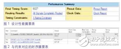
“Design meets timing requirements?†Designers often ask this question each time they complete a design implementation through place and route. Regardless of the answer, designers want to get this information in a straightforward form, as shown in Figure 1.

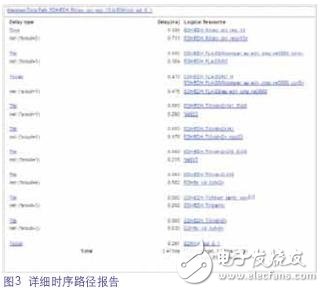
The next question is "How many of the timing requirements are met, and how many have not been reached?" Figure 2 gives a brief summary of the timing results corresponding to each constraint.
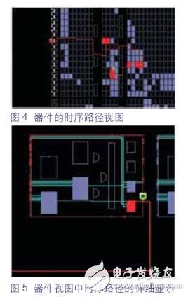
Explore results with different viewsOnce the timing results are presented in summary form, it is also easy to see the details of a particular constraint or path. From the above summary, simply click on a constraint and the designer can see a more detailed timing report, as shown in Figure 3.

Designers can quickly and easily move from high-level timing summaries to detailed textual information to understand specific timing paths.
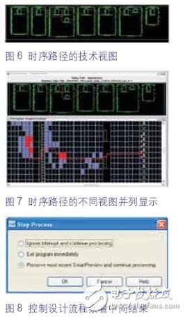
Text information is just one way to understand the timing characteristics of a design. Often, graphic displays are more helpful. For the above design, click on the hyperlink to get a graphical representation of the actual physical implementation of the timing path in the FPGA device, as shown in Figure 4.


The above physical device view is often useful, but other representations are equally useful for understanding the different timing path details in the design. A view based on schematic technology is shown in Figure 6.
In this sequential path view, it is easy to see the number of logical layers in the data path and how the timing path traverses different parts of the design hierarchy. It is also possible to gradually enlarge the displayed schematic to show other logical connections to the cells that make up the path.
Design-centric, not toolsWith multiple views of the same design problem, designers can consider timing issues in different ways and customize the most appropriate solution to the problem. When all of these observation points are integrated into a single design environment, switching between different views is as simple as a click. Sometimes you can display multiple views side by side, as shown in Figure 7.
Provide meaningful intermediate resultsIn the middle of the FPGA design process, it is common to run multiple implementations. For large designs with a large number of timing requirements, it is useful to be able to check intermediate results. By conveniently suspending, detecting, and restoring the implementation process, designers can gain better design visibility during design compilation, as shown in Figure 8.
Imagine that excessive timing constraints may take more time to complete the layout and routing phases of the design implementation. By suspending the process, some designers may think that the design timing is “close enough†that the design can be submitted to the lab for functional debugging. At the same time, after this step, you can restore the layout and continue to optimize to meet the final timing requirements.
More importantly, by examining intermediate results, designers can more quickly determine if there are any timing critical areas and take action as early as possible.
Manage complex source code structuresAs design complexity increases, so does the complexity of the source code structure. Many designers use third-party source code control tools to manage complexity and ensure consistency of source code files. These files are not limited to HDL source files, but also include constraint files, simulation test benchmarks, and more.
Every designer has a unique style and approach to dealing with these issues, so there is no one-size-fits-all solution for all users. By providing a convenient mechanism to determine and selectively output all source code/files in an FPGA design project, designers can use external source control tools that best suit their needs. The output process also includes outputting project information in ASCII form that can later be used to reconstruct the early stages of the project.
ConclusionFor FPGA design productivity, fast timing closure is a key factor. A quick understanding of the design timing state is key to measuring the effectiveness of the FPGA design environment. There are many reasons for timing failures in the timing path, so designers need to have the ability to view timing information from a variety of different perspectives (text and graphics). This way they can make the best decisions on how to improve the design timing. Seamless and transparent synthesis tools will help achieve timing closure quickly
Electric Test Pen ,Battery Detector,Circuit Tester,Voltage Test Pen
YINTE TOOLS (NINGBO) CO., LTD , https://www.yinte-tools.com