In fact, in the chip industry, there is a professional term for dismantling, called reverse engineering. This is actually an open secret of the industry, and many companies are publicly doing this business.
A few days ago, the Guangdong Provincial Procuratorate reported a case of “reverse†R&D chips for profiteering. The responsible person was sentenced to three years in infringement of intellectual property rights. The case was selected by the Supreme People’s Procuratorate for the 2016 “Procuratorial Organs to crack down on IPR crimesâ€. Ten typical cases."
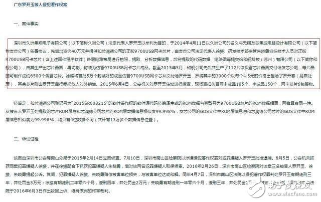
Event review: invested 400,000 yuan to commission imitation NIC chipsAccording to the report of the Procuratorate Daily, Luo Kaiyu is the legal representative of Shenzhen Jiuzhou Jixiang Electronics Co., Ltd., and signed an agreement with Wuxi Youxin Integrated Circuit Design Co., Ltd., which has invested about 400,000 yuan and provided the genuine 9700USB network card of the core and the company. Chip sample.
Xu, the legal representative of Wuxi Company, and the research and development supervisor Zhu, organized technical personnel to extract data information and submitted it to a certain technology company in Suzhou to produce chip wafers, which were then cut and packaged into counterfeit 9700USB network card chips. As of May 2015, Suzhou has produced and delivered 112 of these counterfeit chip wafers, each of which can produce approximately 6,500 counterfeit chips.
Xu delivered the first batch of 50,000 packaged counterfeit 9700USB NIC chips to Luo Kaiyu, and Luo entrusted others to sell it externally, which made huge profits. In June 2015, the police searched Luo Kaiyu's address and seized 105 fake NIC products, 150 semi-finished products, and 6 NIC chips. It has been identified that the ROM layer data extracted from Luo Kaiyu and the ROM layer of the genuine 9700USB NIC chip have a similarity of 99.998%.

The procuratorate believes that reverse engineering technology takes pictures of genuine chips layer by layer, extracts and analyzes the data information, and finally obtains the entire integrated circuit layout structure of the chip, which is a new means of infringing the copyright of computer software. The Nanshan District Court of Shenzhen City sentenced Luo Kaiyu to three years in prison for infringement of copyright and a fine of 50,000 yuan.
The reverse engineering of the chip is explained in detail.Manufacturing is the corresponding disassembly, which is the most violent and direct way to acquire knowledge in the field of chip design. The form in which the chip may be attacked includes the use of infrared rays, chemical delays, and scanning of focused ion beams, with the goal of removing material from the chip and further accessing the IC. It is then possible to use this IC access method to obtain design information, as well as potential data.
In fact, in the chip industry, there is a professional term for dismantling, called reverse engineering. This is actually an open secret of the industry, and many companies are publicly doing this business. In China, the relevant National Defense Electronics Industry Research Institute, various microelectronics research institutes, its important IC design tools are reverse engineering, with a dedicated team and advanced equipment, responsible for dismantling, photography, extraction, analysis, simulation and verification. A set of processes, such as aerospace military FPGAs and analog IC products. For some of the more complex consumer and industrial grade devices, some IC design companies also offer professional reverse engineering services. In Shenzhen, the imitations of various electronic components are numerous, and a complete industrial chain has been formed from the reverse, manufacturing and packaging.

So, what is the reverse engineering of an integrated circuit? How do the various processes work? How is the reverse engineering of these microchips operated and implemented?
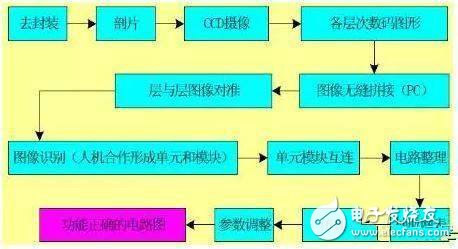
Disassembly: Place the chip to be disassembled in a container filled with concentrated sulfuric acid. The container needs to be covered, but it cannot be tight, so that the gas inside can overflow. Heat the concentrated sulfuric acid in the container to boiling (about 300 degrees Celsius) and apply soda powder around the bottom of the bottle to prevent accidental splashing of sulfuric acid and sulfuric acid.
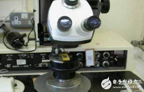
Photographing: Microscopic image acquisition of chip samples layer by layer on a microscopic image automatic acquisition platform. Unlike the reverse design of measuring 3D solids or surfaces, the measurement integrated circuit chip is purely a surface article: put the chip position, focus, select the magnification, make the chip surface visible in the lens and on the display, press the camera button A microscopic image acquisition can be completed. Depending on the size and magnification of the circuit, a layer of circuitry may need to be patched after multiple images are taken, multi-layer circuits need to be aligned after patchwork, and micro-image auto-patch software is used for patchwork and alignment operations.

The microscopic image automatic acquisition platform has a magnification of 1000 times and can enlarge the 0.1 um line to a width of 0.1 mm. This means that it is sufficient to deal with the 0.09um integrated circuit chip currently produced using the most advanced technology.
Referral: The integrated circuit consists of multiple layers, each layer being determined by photolithography using a photomask. The geometry on the mask used to make the integrated circuit is the layout, which is the physical layer corresponding to the integrated circuit.
Now the drawing work can be done by the computer. The mainstream circuit schematic analysis system has powerful functions such as multi-layer microscopic image browsing, circuit unit symbol design, circuit schematic automatic and interactive analysis extraction, and circuit schematic editing. The layout analysis system can complete multi-layer layout contour automatically. Extraction, full-featured layout editing, automatic identification of embedded software code, extraction, verification, and statistics and extraction of design rules.
Finishing: Digital circuits need to be merged with similar graphics, such as NAND gates, NOR gates, flip-flops, etc. The same graphics should not be analyzed multiple times. The proposed circuit is drawn by circuit drawing software (ViewWork, Laker, Cadence, etc.). According to the easy-to-understand circuit layout, other people can also see the function of your extraction circuit. The speed of extracting the circuit is completely determined by the level of experience of the drawing personnel. . Note that the software connects the components according to the position of the layout. If the connection and function of each module are not visible without finishing the circuit, the division and analysis of the circuit function blocks cannot be completed by software.
Analysis: The extracted circuit is organized into a circuit diagram and the geometric parameters (MOS is the width to length ratio) are input. Through your analysis, the circuit function is clear and the circuit connection is correct.
Simulation: Functional simulation verification of the circuit. Analog circuits generally use tools such as Hspice and Cadence, and small-scale digital circuits use tools such as Cadence and Hsim. The circuit is adjusted according to the new process and verified after adjustment.
Verification: Browse, query, edit, debug, and simulate the input schematic. Analyze the circuit principle, adjust the circuit parameters, and observe the output waveform under a certain excitation input to verify the logical correctness of the design. To simulate the extracted netlist and compare it with the pre-imitation results, the layout exports the GDS file and Tape out (transfer the design data to the manufacturer).
Mini Air Purifier,Mini Air Filter,Air Purifier Portable Mini,Mini Purifier
CIXI KYFEN ELECTRONICS CO.,LTD, , https://www.kyfengroup.com